信昌電子陶瓷股份有限公司
Prosperity Dielectrics Co., Ltd.
No.566-1, Kaoshi Rd., Yangmei, Taoyuan 32668, Taiwan (R.O.C.)
Tel : 886-3-4753355
Messrs. :
Date :
Fax : 886-3-4854959
一般共用
2018/05/30
APPROVAL SHEET
Product Name : General Purpose Multilayer Ceramic Chip
Capacitors
Part No. : FN Series
Description : Size 0201~2225, C0G/X7R/X5R/Y5V, UR≤50V
PREPARED BY
APPROVED BY
信昌電子陶瓷股份有限公司
PROSPERITY DIELECTRICS CO., LTD.
桃園市楊梅區高獅路 566-1 號
Tel : 03-4753355 ext :
Contactor :
http://www.pdc.com.tw
Fax : 03-4854959
Mobile :
DCM-003-8.1
Rev 2
�信昌電子陶瓷股份有限公司
Prosperity Dielectrics Co., Ltd.
No.566-1, Kaoshi Rd., Yangmei, Taoyuan 32668, Taiwan (R.O.C.)
Tel : 886-3-4753355
Fax : 886-3-4854959
SPECIFICATION
FOR
Product Name : General Purpose Multilayer Ceramic Chip
Capacitors
Part No. : FN Series
Description : Size 0201~2225, C0G/X7R/X5R/Y5V, UR≤50V
SPEC. No. : FN-000-001-08
DATE : 2018/05/30
DRAWN BY
CHECEKED BY
APPROVED BY
Tsu Chen
Yvens Chou
Joseph Ling
DCM-003-8.2
Rev 2
�信昌電子陶瓷股份有限公司
Prosperity Dielectrics Co., Ltd.
1. INTRODUCTION
POSPERITY Multilayer Ceramic Chip Capacitors supplied in bulk or tape & reel package are ideally
suitable for thick-film hybrid circuits and automatic surface mounting on any printed circuit boards.
The nickel-barrier terminations are consisted of a nickel barrier layer over the silver metallization and then
finished by electroplated solder layer to ensure the terminations have good solderability. The nickel barrier
layer in terminations prevents the dissolution of termination when extended immersion in molten solder at
elevated solder temperature.
2. FEATURES
3. APPLICATIONS
a. A wide selection of sizes is available (0201 to 2225).
b. High capacitance in given case size.
c. Capacitor with lead-free termination (pure Tin).
d. RoHS & HALOGEN compliant.
a. For general digital circuit.
b. For power supply bypass capacitors.
c. For consumer electronics.
d. For telecommunication.
e. DC to DC converter.
4. HOW TO ORDER
FN
PDC
Family
Table 1
21
X
Size
471
K
500
Rated
Voltage
Table 6
Dielectric Capacitance Tolerance
Table 2
Table 3
Table 4
Table 5
P
X
Packaging Thickness
Table 7
Table 6
Table 8
G
Control
Code
Table 9
Table 1
PDC Family
Code
Description
Code
Description
Code
Description
Code
Description
FN
General purpose product ≤50Vdc
4R0
4.0Vdc
100
10Vdc
250
25Vdc
6R3
6.3Vdc
160
16Vdc
500
50Vdc
Table 2
General Purpose
Code
Description
Code
Description
Code
Description
03
15
18
0201 (0603)
0402 (1005)
0603 (1608)
31
32
42
1206 (3216)
1210 (3225)
1808 (4520)
46
52
55
1825 (4563)
2211 (5728)
2220 (5750)
21
0805 (2012)
43
1812 (4532)
56
2225 (5763)
Table 3
Dielectric Material Characteristics
Rated Voltage
Table 7
Packaging Type
Code
Description
Code
Description
B
Bulk
T
Tray package
Code
Description
Code
Description
E
Tape and 7” Reel, Embossed Tape
P
Tape and 7” Reel, Paper Tape
N
C0G
X
X7R
K
Tape and 10” Reel, Embossed Tape
D
Tape and 10” Reel, Paper Tape
B
X5R
F
Y5V
L
Tape and 13” Reel, Embossed Tape
G
Tape and 13” Reel, Paper Tape
Table 4
Capacitance Rule Code
Table 8
Thickness Description
Code
Description
Code
Description
Code
Description
Code
Description
Code
Description
R47
0R5
100
0.47pF
0.5pF
100=10x100=10pF
102
104
106
102=10x102=1000pF
104=10x104=100nF
106=10x106=10µF
A
B
C
0.60 ± 0.10 mm
1.25 ± 0.20 mm
1.25 ± 0.10 mm
0.50 ± 0.20 mm
Q
R
S
0.50 +0.02/-0.05 mm
0.8 + 0.15/-0.10 mm
I
J
K
D
1.40 ± 0.15 mm
L
0.30 ± 0.03 mm
T
0.85 ± 0.10 mm
Table 5
Tolerance
1.15 ± 0.15 mm
3.10 ± 0.30 mm
0.80 ± 0.07 mm
E
1.60 ± 0.20 mm
M
0.95 ± 0.10 mm
U
0.50 ± 0.10 mm
Code
Description
Code
Description
Code
Description
F
2.00 ± 0.20 mm
N
0.50 ± 0.05 mm
V
0.20 ± 0.02 mm
A
B
±0.05 pF
±0.10 pF
I
J
-10% ~ 0%
±5 %
Q
Z
±0.03 pF
-20% ~ +80%
G
H
2.50 ± 0.30 mm
O
P
3.50 ± 0.20 mm
X
Z
0.80 ± 0.10 mm
C
±0.25 pF
K
±10 %
X
+10% ~ +20%
D
±0.50 pF
L
0% ~ +10%
Table 9
F
±1 %
M
±20 %
Code
Description
G
±2 %
N
-5% ~ +10%
G
RoHS Compliant
H
±3 %
P
±0.02 pF
O
Gold plating (Size≥0603)
2.80 ± 0.30 mm
1.60 +0.3/-0.10 mm
0.25 ± 0.03 mm
Special Control Code
Specification No. : FN-000-001-08
~1~
DCM-003-8.3
Rev 2
�信昌電子陶瓷股份有限公司
Prosperity Dielectrics Co., Ltd.
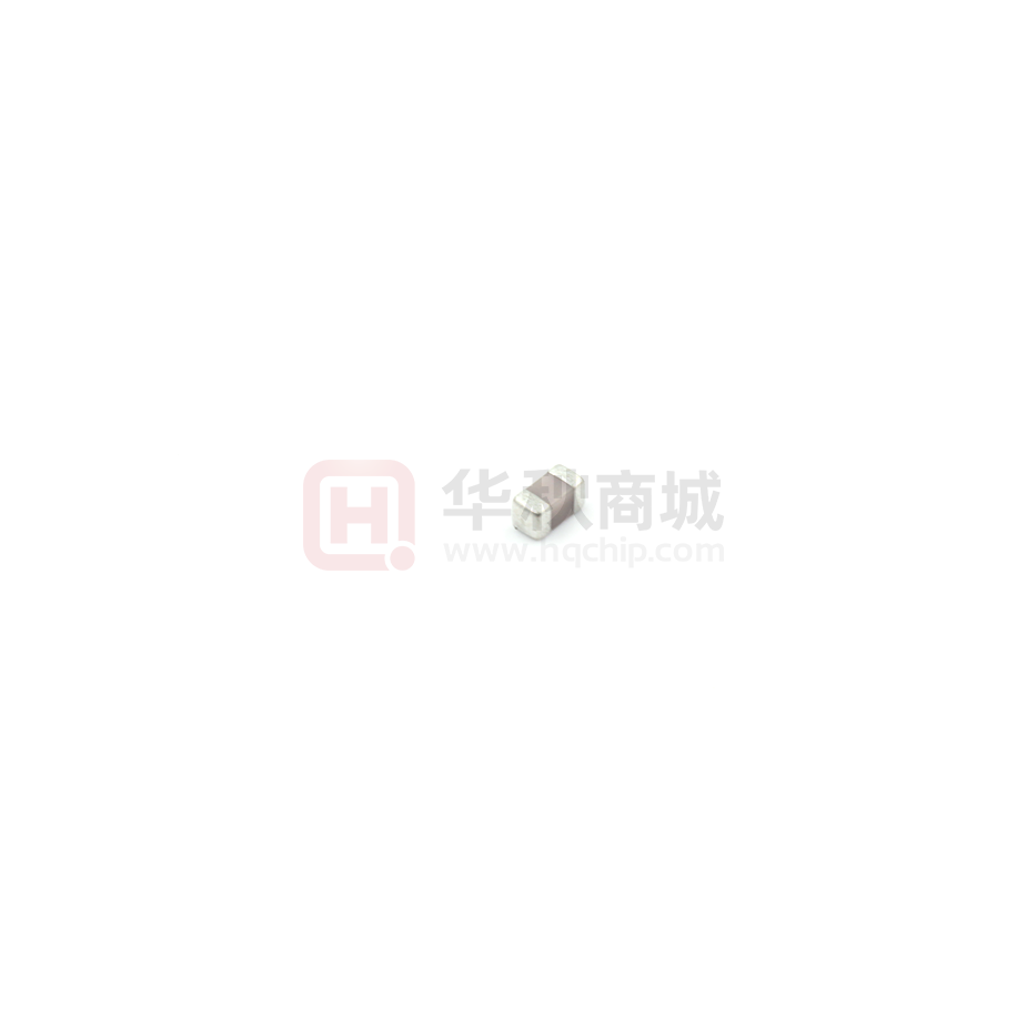
5. EXTERNAL DIMENSIONS
Size Inch (mm)
L (mm)
W (mm)
Code / T (mm)
MB (mm)
0201(0603)
0.60±0.03
0.30±0.03
0.15±0.05
0402(1005)
1.00±0.10
0.50±0.10
0.25 +0.05/-0.10
0603(1608)
1.60±0.15
0.80±0.15
0.40±0.15
0805(2012)
2.00±0.20
1.25±0.20
L
0.50±0.20
See
No.4 Reference
Table 8
1206(3216)
3.20±0.20
1.60±0.20
1210(3225)
3.20±0.30
2.50±0.30
1812(4532)
4.50±0.40
3.20±0.30
0.75±0.35
1825(4563)
4.50±0.40
6.30±0.40
0.75±0.35
2220(5750)
5.70±0.40
5.00±0.40
0.85±0.35
2225(5763)
5.70±0.40
6.30±0.40
0.85±0.35
T
0.60±0.20
0.75±0.35
W
MB
MB
Fig. 5.1 The outline of MLCC
6. GENERAL ELECTRICAL DATA
Dielectric
C0G
Size
Rated voltage (WVDC)
Capacitance range*
Capacitance tolerance**
Tan δ*
Operating temperature
Capacitance characteristic
Termination
X7R
X5R
0201, 0402, 0603, 0805, 0201, 0402, 0603, 0805,
1206, 1210, 1808, 1812, 1206, 1210, 1808, 1812,
0201, 0402, 0603
1825, 2220, 2225
1825, 2220, 2225
6.3V, 10V, 16V,
4V, 6.3V, 10V,
10V, 16V, 25V, 50V
25V, 50V
16V, 25V, 50V
0R1 to 100nF
100pF to 820nF
100pF to 820nF
J(±5% ), K(±10%)
J(±5% ), K(±10%), M(±20%)
Cap.1000pF, 25°C at ambient temperature.
X7R/X5R : Apply 1.0±0.2Vrms, 1.0KHz±10%, at 25°C am bient temperature.
Y5V : Apply 1.0±0.2Vrms, 1.0KHz±10%, at 20°C ambien t temperature.
** Preconditioning for Class II MLCC : Perform a heat treatment at 150±10°C for 1 hour, then leave in ambient condition for 24±2 hours before
measurement.
Y5V
Note 1 : X7R/X5R
Rated
D.F.≤
50V
≤2.5%
35V
25V
16V
≤3.5%
≤3.5%
≤3.5%
10V
≤5%
6.3V
≤10%
4V
≤15%
Exception of D.F.≤
0201(50V), 0603≥0.047µF, 0805≥0.18µF, 1206≥0.47µF,
≤3%
1210≥3.3µF, 1812≥4.7µF, 1825≥4.7µF, 2220≥4.7µF, 2225≥4.7µF
≤5%
0201≥0.01uF, 1210≥4.7µF
≤10%
0402≥0.1µF, 0603>0.1µF, 0805≥1µF, 1206≥2.2µF, 1210≥10µF
≤10%
0603≥1µF, 0805≥2.2µF, 1206≥2.2µF, 1210≥10µF
≤5%
0201≥0.01µF, 0805≥1µF, 1210≥10µF
≤7%
0603≥0.33µF, 1206≥4.7µF
0201≥0.1µF, 0402≥0.10µF, 0603≥0.47µF, 0805≥2.2µF, 1206≥6.8µF,
≤10%
1210≥22µF
≤12.5% 0402≥0.47µF
0201≥0.01µF, 0402≥0.033µF, 0603≥0.15µF, 0805≥0.68µF,
≤5%
1206≥2.2µF, 1210≥4.7µF
0201≥0.1uF(0201/X7R≥0.022µF), 0402≥0.22uF, 0603≥0.68µF,
≤10%
0805≥2.2µF, 1206≥4.7µF, 1210≥22µF
0201≥0.012µF, 0402≥0.33µF(0402/X7R≥0.22µF), 0603≥0.33µF,
≤10%
0805≥2.2µF, 1206≥2.2µF, 1210≥22µF
≤15%
0201≥0.1µF, 0402≥1µF
0201≥0.1µF, 0402≥1µF, 0603≥10µF, 0805≥4.7µF, 1206≥47µF,
≤15%
1210≥100µF
≤20%
0402≥2.2µF
-----
Rated
D.F.≤
50V
≤5%
35V
≤7%
Exception of D.F.≤
≤7%
--≤7%
25V
≤5%
≤9%
16V
≤7%
(C1000pF, 1.0±0.2Vrms, 1KHz±10%.
* Class II : (X7R, X5R, Y5V)
Cap.≤10µF, 1.0±0.2Vrms, 1KHz±10%**.
Cap.>10µF, 0.5±0.2Vrms, 120Hz±20%.
** Test condition : 0.5±0.2Vrms, 1KHz±10%.
X7R :
Q/D.F.
0805=106(6.3V&10V), 0603=475(6.3V).
3. (Dissipation
X6S :
Factor)
0201≥104(6.3V&10V),0402≥225(6.3V),
0402/475(10V), 0603/106(6.3V).
X5R :
01R5≥103, 0201≥224(6.3V,10V,16V)#1,
0402≥475(6.3V,16V), 0402≥225(10V),
0603=106(6.3V,10V).
≤3.5%
≤20%
0603≥0.33µF, 1206≥4.7µF
0201≥0.1µF, 0402≥0.10µF, 0603≥0.47µF,
0805≥2.2µF, 1206≥6.8µF, 1210≥22µF
0402≥0.47µF
0201≥0.01µF, 0402≥0.033µF, 0603≥0.15µF,
0805≥0.68µF, 1206≥2.2µF, 1210≥4.7µF
0201≥0.1uF(0201/X7R≥0.022µF),
0402≥0.22uF, 0603≥0.68µF, 0805≥2.2µF,
1206≥4.7µF, 1210≥22µF
0201≥0.012µF,
0402≥0.33µF(0402/X7R≥0.22µF),
0603≥0.33µF, 0805≥2.2µF, 1206≥2.2µF,
1210≥22µF
0201≥0.1µF, 0402≥1µF
0201≥0.1µF, 0402≥1µF, 0603≥10µF,
0805≥4.7µF, 1206≥47µF, 1210≥100µF
0402≥2.2µF
---
---
≤10%
≤12.5%
≤5%
16V
≤3.5%
≤10%
10V
≤5%
≤10%
≤15%
6.3V
≤10%
4V
≤15%
≤15%
* Y5V
Rated
D.F.≤
Exception of D.F.≤
50V
≤5%
≤7%
0603≥0.1µF, 0805≥0.47µF, 1206≥4.7µF
≤12.5% 1210≥6.8µF
35V
≤7%
---
25V
≤5%
≤7%
≤9%
16V
≤7%
(C30pF, Q≥350.
Y5V
16V
C≥0.47µF
10pF≤Cap.≤30pF, Q≥275+2.5C.
X7R
≥50V
C≥0.082µF
Cap.0.01µF, 0603≥1µF, 0805≥1µF, 1206≥4.7µF,
X5R/X7R/X7S/X6S ≤100V
C≥1.0µF
1210
X7R
>100V
C≥0.22µF
1210≥4.7µF
≤50V
C≥4.7µF
35V : 0603≥1µF, 0805≥2.2µF, 1206≥2.2µF, 1210≥10µF
1812
X7R
100V
C≥1.0µF
≥1GΩ or
25V : 0201≥0.1uF, 0402≥0.22µF, 0603≥2.2µF,
200V~250V
C≥0.47µF
0805≥2.2µF, 1206≥10µF, 1210≥10µF
RxC≥10Ω-F
1825
2220
X7R
≥100V
C≥1.0µF
16V : 0201≥0.1uF, 0402≥0.22µF, 0603≥1µF, 0805≥2.2µF, , whichever
2225
is smaller
1206≥10µF, 1210≥47µF
10V : 0201≥47nF, 0402≥0.47µF, 0603≥0.47µF,
0805≥2.2µF, 1206≥4.7µF, 1210≥47µF
* Test time : 1000 +24/-0 hrs.
6.3V;
4V; Size≥1812
* Before initial measurement (Class II only) : To apply
de-aging at 150°C for 1hr then set for 24±2 hrs at
room temp.
* Measurement to be made after keeping at room
temp. for 24±2 hrs (Class I) or 48±4 hrs (Class II).
** De-rating conditions :
Specification No. : FN-000-001-08
~ 13 ~
DCM-003-8.3
Rev 2
�信昌電子陶瓷股份有限公司
Prosperity Dielectrics Co., Ltd.
8. RELIABILITY TEST CONDITIONS AND REQUIREMENTS
No.
Item
Adhesive
13. Strength of
Termination
Test Condition
Requirements
* Capacitors mounted on a substrate. A force of
2N(0201) or 5N(0402~0603) or 10N(>0603) applied
perpendicular to the place of substrate and parallel
the line joining the center of terminations for 10±1
second.
* No remarkable damage or removal of the terminations.
* The middle part of substrate shall be pressurized by
means of the pressurizing rod at a rate of about 1mm
per second until the deflection becomes 1mm.
14. Bending Test
* No remarkable damage.
Dielectric
Cap. Change
C0G
Within ±5.0% or ±0.5pF, whichever is larger
X7R, X5R
Within ±12.5%
Y5V
Within ±30%
(This capacitance change means the change of capacitance under
specified flexure of substrate from the capacitance measured before the
test)
Unit : mm
15.
Vibration
Resistance
* Vibration frequency : 10~55 Hz/min.
* Total amplitude : 1.5mm.
* Test time : 6 hrs. (Two hrs each in three mutually
perpendicular directions)
* Before initial measurement (Class II only) : To apply
de-aging at 150°C for 1hr then set for 24±2 hrs at
room temp.
* Measurement to be made after keeping at room
temp. for 24±2 hrs (Class I) or 48±4 hrs (Class II).
* No remarkable damage.
* Cap. change and D.F. : To meet initial spec.
Specification No. : FN-000-001-08
~ 14 ~
DCM-003-8.3
Rev 2
�信昌電子陶瓷股份有限公司
Prosperity Dielectrics Co., Ltd.
9. PACKAGE DIMENSION AND QUANTITY
Size
0201(0603)
0402(1005)
0603(1608)
0805(2012)
1206(3216)
1210(3225)
1808(4520)
1812(4532)
1825(4563)
2220(5750)
2225(5763)
Thickness (mm)
0.30±0.03
0.30±0.05
0.30±0.09
0.50±0.05
0.50 +0.02/-0.05
0.50±0.20
0.50±0.10
0.80±0.07
0.80 +0.15/-0.10
0.50±0.10
0.60±0.10
0.80±0.10
0.85±0.10
1.25±0.10
1.25±0.20
0.80±0.10
0.85±0.10
0.95±0.10
1.15±0.15
1.25±0.10
1.60±0.20
1.60 +0.30/-0.10
0.85±0.10
0.95±0.10
1.25±0.10
1.60±0.20
2.00±0.20
2.50±0.30
1.25±0.10
1.60±0.20
2.00±0.20
1.25±0.10
1.60±0.20
2.00±0.20
2.50±0.30
2.80±0.30
1.60±0.20
2.00±0.20
2.50±0.30
2.80±0.30
1.60±0.20
2.00±0.20
2.50±0.30
2.80±0.30
1.60±0.20
2.00±0.20
2.50±0.30
2.80±0.30
Paper tape
7” reel
15k
15k
15k
10k
10k
10k
4k
4k
4k
4k
4k
4k
4k
4k
4k
-
Plastic tape
13” reel
70k
50k
50k
15k
15k
15k
15k
15k
15k
15k
15k
-
7” reel
3k
3k
3k
3k
3k
2k
2k
3k
3k
3k
2k
1k
1k
2k
2k
1k
1k
1k
1k
0.5k
0.5k
1k
1k
0.5k
0.5k
1k
1k
0.5k
0.5k
1k
1k
0.5k
0.5k
13” reel
10k
10k
10k
10k
10k
10k
9k
10k
10k
10k
6k
6k
10k
8k
6k
5k
3k
Unit : pcs
Specification No. : FN-000-001-08
~ 15 ~
DCM-003-8.3
Rev 2
�信昌電子陶瓷股份有限公司
Prosperity Dielectrics Co., Ltd.
9. PACKAGE DIMENSION AND QUANTITY
9.1. EMBOSSED TAPE DIMENSIONS
Fig. 9.1 The dimension of paper tape
Size
Chip
Thickness
A0
B0
T
K0
W
P0
10xP0
P1
P2
D0
D1
E
F
Unit :
0201
0402
0.50±0.05
0.50±0.10
0.70±0.20
1.20±0.20
≤0.80
8.00±0.10
4.00±0.10
40.00±0.10
2.00±0.05
2.00±0.05
1.55±0.05
1.75±0.05
3.50±0.05
mm
0.30±0.03
0.39±0.07
0.69±0.07
≤0.50
8.00±0.10
4.00±0.10
40.00±0.10
2.00±0.05
2.00±0.05
1.55±0.05
1.75±0.05
3.50±0.05
mm
Size
Fig. 9.2 The dimension of plastic tape
0603
0.80±0.07
0.80 +0.15/-0.1
0.80±0.10
1.00 +0.05/-0.1
1.80±0.10
0.95±0.05
8.00±0.10
4.00±0.10
40.00±0.20
4.00±0.10
2.00±0.05
1.55±0.05
1.75±0.05
3.50±0.05
mm
1.02 +0.05/-0.1
1.80±0.10
0.97±0.05
8.00±0.10
4.00±0.10
40.00±0.20
4.00±0.10
2.00±0.05
1.55±0.05
1.75±0.05
3.50±0.05
mm
1.50±0.10
2.30±0.10
0.95±0.05
8.00±0.10
4.00±0.10
40.00±0.20
4.00±0.10
2.00±0.05
1.55±0.05
1.75±0.05
3.50±0.05
mm
1206
Chip
Thickness
0.80±0.10
A0
B0
T
K0
W
P0
10xP0
P1
P2
D0
D1
E
F
Unit :
2.00±0.10
3.50±0.10
0.95±0.05
8.00±0.10
4.00±0.10
40.00±0.20
4.00±0.10
2.00±0.05
1.55±0.05
1.75±0.10
3.50±0.05
mm
0805
1210
0.95±0.10
1.25±0.10
1.60±0.20
1.60+0.3/-0/1