Sunlord Business categories:Level 0(general confidential) Specifications for Wire Wound SMD Power Inductor Page 1 of 12
Rev.10
S P E C I F I C AT I O N S
Customer
Product Name
Wire Wound SMD Power Inductor
Sunlord Part Number
SWPA4030S331MT
Customer Part Number
[
New Released,
Revised]
SPEC No.: SWPA1002220020
【This SPEC is total 12 pages.】
【ROHS Compliant Parts】
Approved By
Checked By
Issued By
Shenzhen Sunlord Electronics Co., Ltd.
Address: Sunlord Industrial Park, Dafuyuan Industrial Zone, Baoan, Shenzhen, China
Tel: 0086-755-29832333
Fax: 0086-755-82269029
【For Customer approval Only】
Qualification Status:
Approved By
Comments:
Full
E-Mail: sunlord@sunlordinc.com
Date:
Restricted
Verified By
Rejected
Re-checked By
Checked By
518110
�Sunlord Business categories:Level 0(general confidential) Specifications for Wire Wound SMD Power Inductor Page 2 of 12
Rev.10
【Version change history】
Rev.
Effective Date
01
Jun.09,2022
Changed Contents
New released
Change Reasons
Approved By
/
Qintian Hou
�Sunlord Business categories:Level 0(general confidential) Specifications for Wire Wound SMD Power Inductor Page 3 of 12
Rev.10
Caution
All products listed in this specification are developed, designed and intended for use in general electronics equipment. The
products are not designed or warranted to meet the requirements of the applications listed below, whose performance and/or
quality require especially high reliability, or whose failure, malfunction or trouble might directly cause damage to society, person,
or property. Please understand that we are not responsible for any damage or liability caused by use of the products in any of
the applications below. Please contact us for more details if you intend to use our products in the following applications.
1. Aircraft equipment
2. Aerospace equipment
3. Undersea equipment
4. nuclear control equipment
5. military equipment
6. Power plant equipment
7. Medical equipment
8. Transportation equipment (automobiles, trains, ships,etc.)
9. Traffic signal equipment
10. Disaster prevention / crime prevention equipment
11. Data-processing equipment
12. Applications of similar complexity or with reliability requirements comparable to the applications listed in the above
�Sunlord Business categories:Level 0(general confidential) Specifications for Wire Wound SMD Power Inductor Page 4 of 12
Rev.10
1
2
Scope
This specification applies to the SWPA4030S331MT of wire wound SMD power inductor.
Product Description and Identification (Part Number)
1) Description:
SWPA4030S331MT of Wire wound SMD power inductor.
2) Product Identification (Part Number)
SWPA
①
4030
②
①
S
③
331
④
M
⑤
T
⑥
②
Type
External Dimensions(L×W×H) [mm]
4030
Wire wound SMD power
4.0X4.0X 3.0
SWPA
inductor
③
S
⑤
Standard Type
Nominal Inductance
Example
Example
331
330uH
Inductance Tolerance
M
⑥
±20%
Packing
T
3.
④
Feature type
Tape Carrier Package
Shape and Dimensions
Dimensions and recommended PCB pattern for reflow soldering, please see Fig.3-1, Fig. 3-2 and Table 3-1.
C
D
a
E
F
c
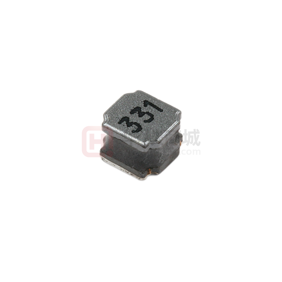
Marking
331
100
A
E
B
D
b
b
Fig.3-1
A
B
C
D
E
F
a
b
c
SWPA4030S
4.0±0.2
4.0±0.2
3.0Max.
3.3±0.2
0.95±0.2
2.1±0.2
1.9Typ.
1.1Typ.
3.7Typ.
Δf
Series
Fig.3-2
Δf: Clearance between terminal and the surface of plate must be 0.1mm max when coil is placed on a flat plate.
4.
Electrical Characteristics
Please refer to Item 6.
1) Operating and storage temperature range (individual chip without packing): -40℃ ~ +125℃(Including Self-heating)
2) Storage temperature range (packaging conditions): -10℃~+40℃ and RH 70% (Max.)
5.
Test and Measurement Procedures
5.1 Test Conditions
5.1.1 Unless otherwise specified, the standard atmospheric conditions for measurement/test as:
�Sunlord Business categories:Level 0(general confidential) Specifications for Wire Wound SMD Power Inductor Page 5 of 12
Rev.10
a. Ambient Temperature: 20±15℃
b. Relative Humidity: 65±20%
c. Air Pressure: 86kPa to 106kPa
5.1.2 If any doubt on the results, measurements/tests should be made within the following limits:
a. Ambient Temperature: 20±2℃
b. Relative Humidity: 65±5%
c. Air Pressure: 86kPa to 106kPa
5.2 Visual Examination
Inspection Equipment: Visual.
5.3 Electrical Test
5.3.1 Inductance (L)
a. Refer to Item 6.Test equipment: WK3260B LCR meter or equivalent.
b. Test Frequency and Voltage: refers to Item 6.
5.3.2 Direct Current Resistance (DCR)
a.
Refer to Item 6.
b. Test equipment: HIOKI 3540 or equivalent.
5.3.3 Saturation Current (Isat)
a. Refer to Item 6.
b. Test equipment: WK3260B LCR meter or equivalent.
5.3.4 Temperature rise current (Irms)
a. Refer to Item 6.
b. Test equipment (see Fig. 5.3.4-1, Fig. 5.3.4-2): Electric Power, Electric current meter, Thermometer.
c. Measurement method
1. Set test current to be 0 mA.
2. Measure initial temperature of choke surface.
3. Gradually increase current and measure choke temperature for corresponding current.
4. Definition of Temperature rise current: DC current that causes the temperature rise (△ T) from ambient temperature
Thermometer
Electric
Power
Electric
Current Meter
RT+△T
RT
0
Idc (A)
Rated current
Fig. 5.3.4-1
Fig. 5.3.4-2
5.3.5 Self-resonant frequency(SRF)
a. Refer to Item 6.
b. Test equipment: Agilent E4991A+16197or equivalent
6.
Electrical Characteristics
Inductance
Customer
Part Number
Min.
Saturation
Heat Rating
Current
Current
DC Resistance
Self-resonant
P/N
Marking
0.1MHz/1V
frequency
Max.
Typ.
Max.
Typ.
Max.
Typ.
Units
μH
MHz
Ω
Ω
A
A
A
A
Symbol
L
SRF
SWPA4030S331MT
330±20%
2.7
DCR
5.20
Isat
4.00
0.30
Irms
0.40
0.25
0.26
331
Note:※1 : Rated current: Isat (max.) or Irms (max.), whichever is smaller;
※2 : Saturation Current: Max. Value, DC current at which the inductance drops less than 30% from its value without current;
Typ. Value, DC current at which the inductance drops 30% from its value without current;
※3 : Irms: DC current that causes the temperature rise (ΔT) from 20°C ambient.
For Max. Value, ΔT<40℃;for Typ. Value, ΔT is approximate 40℃.
The part temperature (ambient + temp. rise) should not exceed 125 °C under worst case operating conditions. Circuit design, component
placement, PCB trace size and thickness, airflow and other cooling provisions all affect the part temperature. Part temperature should be verified
in the end application.
�Sunlord Business categories:Level 0(general confidential) Specifications for Wire Wound SMD Power Inductor Page 6 of 12
Rev.10
Typical Electrical Characteristics:
7.
Structure
The structure of SWPA4030S product, please refer to Fig.7-1 and Table 7-1.
[Table 7-1]
No.
Components
Material
①
Ferrite Core
Ni-Zn Ferrite
②
Wire
Polyurethane system enameled copper wire
③
Magnetic Glue
Epoxy resin and magnetic powder
④
Electrodes
Sn Alloy
Fig.7-1
8.
Product Marking
Please refer to Fig. 8-1.
The content of marking please refers to Item 6.
331
100
Fig 8
. -1
�Sunlord Business categories:Level 0(general confidential) Specifications for Wire Wound SMD Power Inductor Page 7 of 12
Rev.10
9.
Reliability Test
Items
Requirements
No removal or split of the termination or other defects shall
occur.
9.1
Terminal
Test Methods and Remarks
①
Y direct
Strength
X direct
②
③
Solder the inductor to the testing jig (glass epoxy board
shown in Fig.9.1-1) using eutectic solder. Then apply a
force in the direction of the arrow.
10N force.
Keep time: 5s
Fig.9.1-1
9.2
Resistance
Flexure
No visible mechanical damage.
①
to
②
③
④
⑤
⑥
Solder the chip to the test jig (glass epoxy board) using
eutectic solder. Then apply a force in the direction
shown as Fig.9.2-1.
Flexure: 2mm
Pressurizing Speed: 0.5mm/sec
Keep time: 30±1s
Test board size: 100X40X1.0
Land dimension:
Please see Fig.3-1
Fig.9.2-1
9.3
Vibration
①
②
No visible mechanical damage.
Inductance change: Within ±10%
①
②
③
Solder the chip to the testing jig (glass epoxy board
shown as the following figure) using eutectic solder.
The chip shall be subjected to a simple harmonic
motion having total amplitude of 1.5mm, the frequency
being varied uniformly between the approximate limits
of 10 and 55 Hz.
The frequency range from 10 to 55 Hz and return to 10
Hz shall be traversed in approximately 1 minute. This
motion shall be applied for a period of 2 hours in each
3 mutually perpendicular directions (total of 6 hours).
9.4
Temperature
coefficient
Inductance change: Within ±20%
①
②
Temperature: -40℃~+125℃
With a reference value of +20℃, change rate shall be
calculated
9.5
Solder ability
90% or more of electrode area shall be coated by new
solder.
①
The test samples shall be dipped in flux, and then
immersed in molten solder.
Solder temperature: 245±5℃
Duration: 5±1 sec.
Solder: Sn/3.0Ag/0.5Cu
Flux: 25% resin and 75% ethanol in weight
Immersion depth: all sides of mounting terminal shall
be immersed
②
③
④
⑤
⑥
9.6
Resistance to
Soldering Heat
① No visible mechanical damage.
② Inductance change: Within ±10%
①
②
③
④
Re-flowing Profile: Please refer to Fig. 9.6-1.
Test board thickness: 1.0mm
Test board material: glass epoxy resin
The chip shall be stabilized at normal condition for 1~2
hours before measuring
Peak 260℃ max
260℃
217℃
Max Ramp Up Rate=3℃/sec.
Max Ramp Down Rate=6℃/sec.
60~90sec.
200
150
℃
℃
25℃
60~120sec.
Time 25℃ to Peak =8 min max
Fig. 9.6-1
�Sunlord Business categories:Level 0(general confidential) Specifications for Wire Wound SMD Power Inductor Page 8 of 12
Rev.10
①
②
9.7
Thermal Shock
30 min.
125℃
②
③
④
30 min.
Ambient
Temperature
Temperature and time: -40±3℃ for 30±3 min→125℃
for 30±3min, please refer to Fig. 9.7-1.
Transforming interval: Max. 20 sec
Tested cycle: 100 cycles
The chip shall be stabilized at normal condition for
1~2 hours before measuring
①
No visible mechanical damage.
Inductance change: Within ±10%
30 min.
-40℃
20sec. (max.)
Fig.9.7-1
9.8
Resistance to Low
Temperature
①
②
9.9
Resistance to High
Temperature
①
②
9.10
Damp Heat
①
②
9.11
Loading Under
Damp Heat
9.12
Loading at High
Temperature
Temperature: -40±3℃
Duration: 1000±24 hours
The chip shall be stabilized at normal condition for
1~2 hours before measuring
①
②
③
Temperature: 125±2℃
Duration: 1000±24 hours
The chip shall be stabilized at normal condition for
1~2 hours before measuring.
No mechanical damage.
Inductance change: Within ±10%
①
②
③
④
Temperature: 60±2℃
Humidity: 90% to 95%RH
Duration: 1000±24 hours
The chip shall be stabilized at normal condition for
1~2 hours before measuring
①
②
No mechanical damage.
Inductance change: Within ±10%
①
②
③
④
⑤
Temperature: 60±2℃
Humidity: 90% to 95% RH
Applied current: Rated current
Duration:1000±24 hours
The chip shall be stabilized at normal condition for
1~2 hours before measuring
①
②
No mechanical damage.
Inductance change: Within ±10%
①
②
③
④
Temperature: 85±2℃
Applied current: Rated current
Duration: 1000±24 hours
The chip shall be stabilized at normal condition for
1~2 hours before measuring
No mechanical damage.
Inductance change: Within ±10%
Packaging, Storage and Transportation
10.1 Tape and Reel Packaging Dimensions
10.1.1 Taping Dimensions (Unit: mm)
Please refer to Fig. 10.1.1 and Table 10.1.1.
P2
T
B0
F
D0
K0
P0
E
P1
W
10.
①
②
③
No visible mechanical damage
Inductance change: Within ±10%
A0
Fig. 10.1.1
[Table 10.1.1]
Series
A0
B0
W
E
F
P0
P1
P2
D0
T
K0
SWPA4030S
4.3±0.1
4.3±0.1
12.0±0.3
1.75±0.1
5.5±0.1
4.0±0.1
8.0±0.1
2.0±0.1
1.5+0.1/-0.0
0.4±0.03
3.2±0.1
10.1.2 Direction of rolling
Please refer to Fig. 10.1.2
�Sunlord Business categories:Level 0(general confidential) Specifications for Wire Wound SMD Power Inductor Page 9 of 12
331
331
331
331
Rev.10
10.1.3 Reel Dimensions (Unit: mm)
Please refer to Fig. 10.1.3.
12.4+0.2/0.0m m
Ø330
Ø 13 .0+ 0.2/-0.0
10.75±0.2
Ø100
2.3±0 .2
M ax< 18.4 m m
10.1.4 Top tape strength
F Ig .10.1.3 -1
165°~180 °
Peel-off strength: 10~100gf.
Peel-off angle: 165°~180°, refers to Fig.10.1.4.
Peel-off speed: 300mm/min.
Top cover tape
10.1.5 The number of components
Fig. 10.1.4
A tape & reel package contains 2000 inductors.
10.1.6 The allowable number of empty chip cavities
Maximum two (2) chip cavities missing product may exist in a reel but they may not be consecutive two cavities.
10.2 Packing Documents and Marking
10.2.1 Packing Documents
Packing documents include the following:
1)
Packaging list
Fig.10.2.3-2A
2)
Certificate of compliance (COC)
10.2.2 Packing QTY.
1)
Inner Box: 1 reel in each box.
2)
Outer Box:2 or 4 inner boxes in each outer case.
Fig.10.2.3-2B
3)
2 or 4 reels in each outer case.
10.2.3 Marking
1)Marking label information on reels includes (see Fig.10.2.3-1、 Fig.10.2.3-2A/2B):
Fig.10.2.3-2A: Shipping labels
a).
P/O No.
b). Customer Part No.
c). Sunlord Part No.
d). Quantity..
e). Lot No.
f).
Date code
Fig.10.2.3-1
�Sunlord Business categories:Level 0(general confidential) Specifications for Wire Wound SMD Power Inductor Page 10 of 12
Rev.10
g). Inspection stamp
h). MFG address as ‘Made In China’.
Fig.10.2.3-2B: Production labels
a) . P/O No.
b). Quantity..
c). Lot No.
d). Inspe No
e). Inspection stamp
f).
MFG address as ‘Made In China’.
g). sequence number
Fig.10.2.3-2A
Fig.10.2.3-3
[Table 10.2.3-1]
Packaging type
Inner box
A(mm)
B(mm)
C(mm)
340
30
340
[Table 10.2.3-2]
Fig.10.2.3-2B
Packaging
L(mm)
W(mm)
1)Marking label information on inner box
type
a). Inner box please refers to Fig.10.2.3-3and Table 10.2.3-1
Type1
380
380
b). Marking Label on inner box
N/A
Type2
380
380
2)Marking on outer case (see Fig.10.2.3-4~6 ):
Out case size pleases reefers to Table 10.2.3-2.
a). Manufacturer: Sunlord ID:
L
“Shenzhen Sunlord Electronics Co., Ltd.”
W
b). Packing label include the following:
i)
Customer
ii)
Manufacturer
iii)
Date code
Fig. 10.2.3-6
iv)
C/No.
Outer
Case
Example; “1/10” means that this case is the 1st one
H
Of total 10 cases
Fig. 10.2.3-5
v)
P/O No.
Shenzhen Sunlord Electronics Co., Ltd.
vi)
Customer Part No.
vii)
Sunlord Part No.
Fig. 10.2.3-4
viii)
Quantity.
ix)
Inspection Stamp.
Customer
C/No.
Fig.10.2.3-5
Fig.10.2.3-6
H(mm)
250
190
�Sunlord Business categories:Level 0(general confidential) Specifications for Wire Wound SMD Power Inductor Page 11 of 12
Rev.10
11.
Visual inspection standard of product
File No:
Applied to Wire Wound SMD Power Inductor Series
REV:01
Effective date:
No.
Defect Item
Graphic
1
Core defect
The defect length/width (l or w) more than L/6 or W/6, NG.
AQL=0.65
2
Core crack
Visual cracks, NG.
AQL=0.65
3
Starvation
①
②
③
AQL=0.65
Rejection identification
Resin starved length, l, more than L/2, NG.
IF W>2mm, resin starved width, w, more than W/2, NG.
IF W≤2mm, resin starved width, w, don't control.
Acceptance
4
Excessive
glue
The length, width or height of product beyond specified value,
NG.
AQL=0.65
5
Cold solder
Cold solders l more than1mm, NG.
AQL=0.65
H
6
①
②
Solder icicle
The height H of product beyond specified value, NG;
The clearance Δf beyond specified value listed in Item 5,
NG;
AQL=0.65
Δf
f
7
Electrode
uneven
The clearance Δf beyond specified value listed in Item 5, NG;
0.2mm Max
Δf
AQL=0.65
�Sunlord Business categories:Level 0(general confidential) Specifications for Wire Wound SMD Power Inductor Page 12 of 12
Rev.10
12.
Recommended Soldering Technologies
12.1Re-flowing Profile:
△ Preheat condition: 150 ~200℃/60~120sec.
△ Allowed time above 217℃: 60~90sec.
△ Max temp: 260℃
△ Max time at max temp: 5sec.
△ Solder paste: Sn/3.0Ag/0.5Cu
△ Allowed Reflow time: 2x max
Please refer to Fig. 12.1-1.
[Note: The reflow profile in the above table is only for
qualification and is not meant to specify board assembly
profiles. Actual board assembly profiles must be based on
the customer's specific board design, solder paste and
process, and should not exceed the parameters as the
Reflow profile shows.]
12.2 Iron Soldering Profile:
△ Iron soldering power: Max. 30W
△ Pre-heating: 150℃/60sec.
△ Soldering Tip temperature: 350℃ Max.
△ Soldering time: 3sec. Max.
△ Solder paste: Sn/3.0Ag/0.5Cu
△ Max.1 times for iron soldering
Please refer to Fig. 12.2-1.
[Note: Take care not to apply the tip of
the soldering iron to the terminal electrodes.]
Peak 260℃ max
260℃
Max Ramp Up Rate=3℃/sec.
217℃
Max Ramp Down Rate=6℃/sec.
60~90sec.
200℃
150℃
60~120sec.
25℃
Time 25℃ to Peak =8 min max
Fig. 12.1-1.
3sec. Max.
350℃
Soldering Iron
Power: max. 30W
Diameter of Soldering
Iron 1.0mm max.
Tc ℃
Fig. 12.2-1.
13.
Precautions
13.1 Surface mounting
Mounting and soldering condition should be checked beforehand.
Applicable soldering process to this product is reflow soldering only.
Recommended conditions for repair by soldering iron:
Preheat the circuit board with product to repair at 150℃ for about 1 minute.
Put soldering iron on the land-pattern.
Soldering iron’s temperature: 350℃ maximum/Duration: 3 seconds maximum/1 time for each terminal.
The soldering iron should not directly touch the inductor.
Product once removes from the circuit board may not be used again.
13.2 Handing
Keep the products away from all magnets and magnetic objects.
Be careful not to subject the products to excessive mechanical shocks.
Please avoid applying impact to the products after mounted on pc board.
Avoid ultrasonic cleaning.
13.3 Storage
To maintain the solderability of terminal electrodes and to keep the packing material in good condition, temperature and
humidity in the storage area should be controlled.
Recommended conditions: -10℃~40℃, 70%RH (Max.)
Even under ideal storage conditions, solderability of products electrodes may decrease as time passes. For this reason,
product should be used with one year from the time of delivery.
In case of storage over 6 months, solderability shall be checked before actual usage.
13.4 Regarding Regulations
Any Class-Ⅰor Class-Ⅱ ozone-depleting substance (ODS) listed in the Clean Air Act in US for regulation is not included in the
products or applied to the products at any stage of whose manufacturing processes.
Certain brominated flame retardants (PBBs,PBDEs) are not used at all.
The products of this specification are not subject to the Export Trade Control Order in China or the Export Administration
Regulations in US.
13.5 Guarantee
The guaranteed operating conditions of the products are in accordance with the conditions specified in this specification.
Please note that Sunlord takes no responsibility for any failure and/or abnormality which is caused by use under other than the
aforesaid operating conditions.
�


 工商网监
湘ICP备2023018690号
工商网监
湘ICP备2023018690号