PJM60N40TE
N-Channel Enhancement Mode Power MOSFET
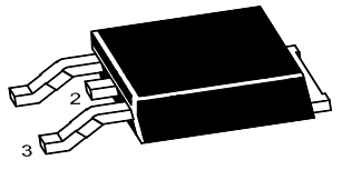
TO-252
Features
⚫ Fast Switching
⚫ Low Gate Charge and RDS(on)
⚫ Low Reverse transfer capacitances
⚫ VDS= 40V,ID= 60A
RDS(on)< 13mΩ @VGS= 10V
1. Gate
2.Drain
3.Sourse
Schematic Diagram
Applications
⚫ Power switching application
2.Drain
⚫ Hard switched and high frequency circuits
⚫ Uninterruptible power supply
1.Gate
3.Source
Absolute Maximum Ratings
Ratings at 25℃ ambient temperature unless otherwise specified.
Parameter
Symbol
Value
Unit
Drain-Source Voltage
VDS
40
V
Gate-Source Voltage
VGS
±20
V
Drain Current-Continuous
ID
60
A
Drain Current-Pulsed Note1
IDM
200
A
Single pulse avalanche energy Note4
EAS
400
mJ
Avalanche energy, Repetitive Note1
EAR
50
mJ
Avalanche Current Note1
IAR
30
A
Maximum Power Dissipation
PD
65
W
Junction Temperature
TJ
175
°C
TSTG
-55 to +175
°C
RθJC
2.3
°C/W
Storage Temperature Range
Thermal Characteristics
Maximum Junction-to-Case Note2
www.pingjingsemi.com
Revision:2.0 May-2021
1/4
�PJM60N40TE
N-Channel Enhancement Mode Power MOSFET
Electrical Characteristics
(Ta=25℃ unless otherwise specified)
Parameter
Symbol
Test Condition
Min.
Typ.
Max.
Unit
Drain-Source Breakdown Voltage
V(BR)DSS
VGS=0V,ID=250μA
40
--
--
V
Zero Gate Voltage Drain Current
IDSS
VDS=40V,VGS=0V
--
--
1
μA
Gate-Body Leakage Current
IGSS
VGS=±20V,VDS=0V
--
--
±1
μA
Gate Threshold Voltage Note3
VGS(th)
VDS=VGS,ID=250μA
1.0
1.6
2.0
V
Drain-Source On-Resistance Note3
RDS(on)
VGS=10V,ID=30A
--
7.5
13
mΩ
gFS
VDS=5V,ID=30A
15
--
--
S
--
1350
--
pF
--
250
--
pF
Static Characteristics
Forward Transconductance Note3
Dynamic Characteristics
Input Capacitance
Ciss
Output Capacitance
Coss
Reverse Transfer Capacitance
Crss
--
200
--
pF
Turn-on Delay Time
td(on)
--
6.5
--
nS
Turn-on Rise Time
tr
VDD=20V, ID=30A
--
17
--
nS
Turn-off Delay Time
td(off)
VGS=10V,RG=3Ω
--
28
--
nS
VDS=20V,VGS=0V,f=1MHz
Switching Characteristics
Turn-off Fall Time
tf
--
16
--
nS
Total Gate Charge
Qg
--
30
--
nC
Gate-Source Charge
Qgs
--
4.7
--
nC
Gate-Drain Charge
Qgd
--
6.5
--
nC
--
--
1.5
V
--
--
60
A
VDD=20V,ID=30A, VGS=10V
Source-Drain Diode Characteristics
Diode Forward Voltage Note3
VSD
Diode Forward Current Note2
IS
VGS=0V,IS=60A
Note: 1. Repetitive Rating: Pulse width limited by maximum junction temperature.
2. Surface Mounted on FR4 Board, t ≤ 10 sec.
3. Pulse Test: Pulse width≤300μs, duty cycle≤2%.
4. EAS condition : Tj=25℃ ,VDD=30V,VG=10V,L=0.5mH,Rg=25Ω.
www.pingjingsemi.com
Revision:2.0 May-2021
2/4
�PJM60N40TE
N-Channel Enhancement Mode Power MOSFET
Typical Characteristic Curves
VGS=3V
Normalized On-Resistance
ID Drain Current (A)
2
VDS=5V
125℃
25℃
TJ Junction Temperature (℃)
VGS Gate-Source Voltage (V)
ID Drain Current (A)
VDS Drain-Source Voltage (V)
ID Drain Current (A)
www.pingjingsemi.com
Revision:2.0 May-2021
VDS=20V
ID=20A
Qg Gate Charge (nC)
IS Reverse Drain Current (A)
RDS(on) On-Resistance (mΩ)
VGS Gate-Source Voltage (V)
VGS=10V
VGS=10V
ID=20A
125℃
25℃
VSD Source-Drain Voltage (V)
3/4
�PJM60N40TE
N-Channel Enhancement Mode Power MOSFET
Package Outline
TO-252
Dimensions in mm
6.6±0.076
2.3±0.076
5.3±0.05
2.3
2.3
2.7±0.10
1
c
0.9±0.05
5
5.6±0.076
1.2±0.05
5
b
0.7±0.10
5
1.0±0.05
a
0.5±0.05
0.50±0.05
A-A
+0.10
0.6-0.05
2-R0.25
0.10±0.05
e
d
1.15±0.10
0.8±0.05
3
A-A
3±
f
www.pingjingsemi.com
Revision:2.0 May-2021
3
4/4
�
很抱歉,暂时无法提供与“PJM60N40TE”相匹配的价格&库存,您可以联系我们找货
免费人工找货