PJ9570 Series
Low Dropout Regulators
Description
SOT-23
3.VIN
The PJ9570 Series are highly precise,low noise,positive voltage LDO regulators
manufactured using CMOS processes. The PJ9570 performance is optimized for
battery-powered systems to deliver ultra low noise and low quiescent current.
Regulator ground current increases only slightly in dropout, further prolonging the
1.GND
2.VOUT
battery life. The PJ9570 Series also works with low-ESR ceramic capacitors,
SOT-23-3
reducing the amount of board space necessary for power applications, critical in
3.VIN
hand-held wireless devices. The PJ9570 Series consumes less than 1μA in
shutdown mode and has fast turn-on time less than 50s. The other features include
ultra low dropout voltage, high output accuracy, current limiting protection, and high
ripple rejection ratio.
Features
1.GND
⚫ Ultra Low Noise for RF Application
2.VOUT
SOT-89
⚫ Ultra Fast Response in Line/Load Transient
2.VIN
⚫ Low Power Consumption:70uA(Typ.)
⚫ PSRR=75dB@1KHz
⚫ Maximum Output Current: 500mA
⚫ Low Dropout : 100mV @ 100mA at VOUT=3.3V
⚫ Operating Voltage Ranges : 2V to 6.5V
1.GND 2.VIN 3.VOUT
⚫ Over Temperature and Current Limiting Protection
⚫ Thermal Shutdown Protection
SOT-23-5
4. NC
5. VOUT
Applications
⚫ Battery-Powered Equipment
⚫ CDMA/GSM Cellular Handsets
⚫ Audio/Video Equipment
1.VIN
Marking Code
9570
-XX
XX:Output Voltage
e.g. 3.0:3.0V 3.3:3.3V
www.pingjingsemi.com
Revision:2.0 Aug-2021
2.GND
3.EN
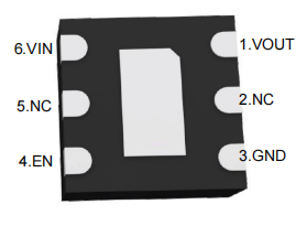
DFN2x2C-6L
6.VIN
1.VOUT
5.NC
2.NC
4.EN
3.GND
1 / 11
�PJ9570 Series
Low Dropout Regulators
Functional Pin Description
Pin Name
Pin Function
EN
Chip Enable (Active High). Note that this pin is high impedance
NC
NO Connected
GND
Ground
VOUT
Output Voltage
VIN
Power Input Voltage
Ordering Information
PJ9570-
Package Type
SA:SOT-23 SC:SOT-23-3
SQ:SOT-89 SE:SOT-23-5
DFC : DFN2x2C-6L
Output Voltage
12 : 1.2V 15 : 1.5V 18 : 1.8V
25 : 2.5V 28 : 2.8V 30 : 3.0V
33 : 3.3V 36 : 3.6V
Output current tap
M : 500mA
Typical Application Circuit
PJ9570
VIN
CIN
1µF
Chip Enable
www.pingjingsemi.com
Revision:2.0 Aug-2021
VIN
VOUT
GND
EN
COUT
1µF
VOUT
NC
2 / 11
�PJ9570 Series
Low Dropout Regulators
Function Block Diagram
www.pingjingsemi.com
Revision:2.0 Aug-2021
3 / 11
�PJ9570 Series
Low Dropout Regulators
Absolute Maximum Ratings Note1
Ratings at 25℃ ambient temperature unless otherwise specified.
Parameter
Value
Unit
-0.3 ~ +7
V
-0.3 ~ +0.3
V
-0.3~VIN+0.3
V
SOT-23
200
mW
SOT-89
400
mW
SOT-23-3
250
mW
SOT-23-5
250
mW
DFN2x2C-6L
560
mW
SOT-23
500
°C/W
SOT-89
250
°C/W
SOT-23-3
400
°C/W
SOT-23-5
400
°C/W
DFN2x2C-6L
180
°C/W
-40 ~ +85
°C
260
°C
-40 ~ +125
°C
ESD(HBM) Note2
4
KV
ESD(CDM) Note2
400
V
VIN,VEN to GND Voltage
VIN
VON/OFF
VOUT to VIN Voltage
Power Dissipation
Thermal Resistance,Junction-to-Ambient
Operating Ambient Temperature
Junction temperature
Storage temperature range
Note 1. Stresses beyond those listed under “Absolute Maximum Ratings” may cause permanent damage to the device.
These are stress ratings only, and functional operation of the device at these or any other conditions beyond those
indicated in the operational sections of the specifications is not implied. Exposure to absolute maximum rating
conditions may affect device reliability.
2. ESD testing is performed according to the respective JESD22 JEDEC standard. The human body model is a 100pF
capacitor discharged through a 1.5KΩ resistor into each pin.The machine model is a 200pF capacitor discharged into
each pin.
Parameter
Supply Voltage
Value
Unit
2 ~ 6.5
V
Operating Junction Temperature Range
TJ
-40 ~ +125
°C
Operating Free Air Temperature Range
TA
-40 ~ +85
°C
www.pingjingsemi.com
Revision:2.0 Aug-2021
4 / 11
�PJ9570 Series
Low Dropout Regulators
Electrical Characteristics
(VIN=VOUT+1, VOUT = 3.3V, CIN=1µF, COUT=1µF, TA=25℃ , unless otherwise noted.)
Parameter
Input Voltage
Symbol
Test Conditions
VIN
Output Voltage Accuracy
Quiescent Current
Min.
Typ.
Max.
Unit
-0.3
--
6.5
V
∆VOUT
IOUT=40mA
-2
--
+2
%
IQ
VIN>VOUT,EN=VIN IOUT=0mA
--
70
--
μA
IOUT=100mA
--
100
--
IOUT=200mA
--
220
--
mV
Dropout Voltage Note1
VDROP
Line Regulation
∆VLINE
VIN=VOUT+1 to 7V,IOUT=40mA
--
0.05
--
%/V
Load Regulation
∆VLOAD
1mA
很抱歉,暂时无法提供与“PJ9570M12DFC”相匹配的价格&库存,您可以联系我们找货
免费人工找货- 国内价格
- 5+1.08983
- 50+0.85569
- 150+0.75546