PJL4115SR
High Brightness Step-Down LED Driver
Description
The PJL4115SR is a high-efficiency step-down LED driver controller with a wide input voltage
range of 6V to 30V. It is designed to operate in continuous current mode.
The PJL4115SR employs a hysteretic control architecture that accurately regulates LED current
with a feedback coming from an external high-side current-sense resistor. This control scheme
optimizes circuit stabilization and fast response time without loop compensation. Its low 200mV
average feedback voltage reduces power loss and improves the converter’s efficiency.
The PJL4115SR implements PWM and analog dimming together through the DIM pin. It also
Includes thermal overload protection in case of output overload.
Features
Wide 6V to 30V Input Range
Able to Drive <1.5A LED Load
High Efficiency
Open LED Protection
No need compensation
Thermal Shutdown
Hysteresis Control
RoHS and Halogen free compliance
Available in SOT-89-5 Package
Applications
Automotive/Decorative LED Lighting
Emergency Lighting
LED Backlighting
Low Voltage Halogen Replacement
Typical Application
www.pingjingsemi.com
Revision: 2.0 Apr-2022
1/9
�PJL4115SR
High Brightness Step-Down LED Driver
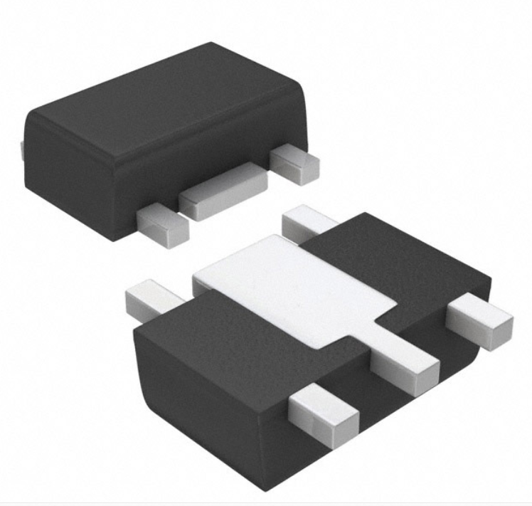
Pin Function And Descriptions
SOT-89-5
5.VIN
4.CSN
4115
1.SW 2.GND 3.DIM
Pin No. Symbol
1
SW
2
GND
3
DIM
4
CSN
5
VIN
www.pingjingsemi.com
Revision: 2.0 Apr-2022
Description
Drain of the internal NMOS
Ground
PWM/Analog Diming Input. Internal weak pull up.
Drive DIM low to turn off the output
Connect sensor input reference to VIN for measure
output current.
Power input
2/9
�PJL4115SR
High Brightness Step-Down LED Driver
Block Diagram
Regulator
UVLO
180mV
220mV
Logic
Driver
Thermal Regulator
Analog/PWM Diming
Absolute Maximum Ratings (at TA = 25°C)
Parameter
Value
Unit
VIN,CSN to GND
-0.3 ~ +36
V
SW to GND
-0.3 ~ +36
V
DIM to GND
-0.3 ~ +6.5
V
RθJA
45
°C/W
TJ
-40 ~ +150
°C
TSTG
-55 ~ +150
°C
Junction to Ambient Thermal Resistance
Operation Junction temperature range
Storage temperature range
www.pingjingsemi.com
Revision: 2.0 Apr-2022
3/9
�PJL4115SR
High Brightness Step-Down LED Driver
Electrical Characteristics
TJ = 25°C, VIN = 12V, unless otherwise noted
Parameter
Input Voltage
Symbol
Test Conditions
VIN
Min.
Typ.
Max.
Unit
6
--
30
V
VCC UVLO Threshold
VUVLOTH
VCC Rising
--
5.5
--
V
VCC UVLO Hysteresis
VUVLOHYS
VCC Falling
--
0.5
--
V
IQ
No Switching
--
270
--
μA
VCS
VIN-CSN
194
200
206
mV
VCS_HY
--
15
--
%
ICSN
--
3
--
μA
VDIM_F
--
3.8
--
V
Quiescent Supply Current
Current Sense Voltage
Current Sense Threshold
CSN Input Current
DIM Floating Voltage
IDIM
VDIM=5V
--
27
--
μA
DIM Pull Up Current
IDIM_PU
VDIM=0V
--
-25
--
μA
DIM Input High
VDIM_H
2.5
--
--
V
DIM Input Low
VDIM_L
--
--
0.3
V
0.5
--
2.5
V
FPWMmin
--
0.1
--
KHz
FPWMmax
--
20
--
KHz
FMAX
--
1
--
MHz
RDS(ON)
--
240
--
mΩ
--
105
--
°C
--
160
--
°C
DIM Input Leakage Current
DIM Voltage Range
Min. Recommended PWM
Dimming Frequency
Max. Recommended PWM
Dimming Frequency
Max. Switch Frequency
MOSFET ON Resistance
VDIM
Thermal Regulate
TREG
Thermal Shutdown
TSH
www.pingjingsemi.com
Revision: 2.0 Apr-2022
VDIM Rising
Temp Rising
4/9
�PJL4115SR
High Brightness Step-Down LED Driver
Typical Characteristic Curves
TA = 25°C, VIN =24V, RCS=0.3Ω, unless otherwise noted
Iout Output Current (A)
100
Efficiency(%)
95
90
85
80
75
70
1LEDs
65
2LEDs
60
6LEDs
0
10
20
Vin Input Votage (V)
1.2
1
0.8
0.6
0.4
0
30
Rcs=0.3Ω
Rcs=0.5Ω
Rcs=0.2Ω
0.2
6
10
14
18
22
26
30
Vin Input Votage (V)
Power ON
Power OFF
(Vin=24V,L=33uH, 4LEDs)
(Vin=24V,L=33uH, 4LEDs)
CH2:Vin 10V/div
CH2:Vin 10V/div
CH3:Vsw 10V/div
CH3:Vsw 10V/div
CH4:Iout 500mA/div
CH4:Iout 500mA/div
Operation waveform
(Vin=12V, L=33uH, 4LEDs)
Operation waveform
(Vin=24V, L=33uH, 4LEDs)
CH4:Iout 500mA/div
CH4:Iout 500mA/div
CH3:Vsw 5V/div
CH3:Vsw 10V/div
www.pingjingsemi.com
Revision: 2.0 Apr-2022
5/9
�PJL4115SR
High Brightness Step-Down LED Driver
PWM Dimming
(Vin=24V, L=33uH, Iout=1A, 4LEDs)
CH1:PWM F=100Hz D=1% 5V/div
PWM Dimming
(Vin=24V, L=33uH, Iout=1A, 4LEDs)
CH1:PWM F=100Hz D=99% 5V/div
CH4:Iout 500mA/div
CH4:Iout 500mA/div
CH3:Vsw 10V/div
CH3:Vsw 10V/div
PWM Dimming
(Vin=24V, L=33uH, Iout=1A, 4LEDs)
PWM Dimming
(Vin=24V, L=33uH, Iout=1A, 4LEDs)
CH1:PWM F=5KHz D=20%5V/div
CH1:PWM F=5KHz D=80% 5V/div
CH4:Iout 500mA/div
CH4:Iout 500mA/div
CH3:Vsw 10V/div
CH3:Vsw 10V/div
www.pingjingsemi.com
Revision: 2.0 Apr-2022
6/9
�PJL4115SR
High Brightness Step-Down LED Driver
Operation
Steady State
The PJL4115SR is a step-down LED-current convertor that is easily configured for a wide
input that ranges from 6V to 30V input. The PJL4115SR uses a High-side current-sense resistor to
detect and regulate LED current. The average voltage across the current- sense resistor is
measured and regulated in the 200mV range.
The internal 1.2V reference voltage provides a 0.5V reference to enable the part. When
VDIM>0.5V, the output of the comparator goes high and enables the other blocks. While the
internal DIM pin weak pull up to 3V
Dimming Control
The PJL4115SR allows the DIM pin to control both Analog and PWM dimming. Whenever the
voltage on DIM is less than 0.3V, the chip turns off. For analog dimming, when the voltage on DIM
is from 0.5V to 2.5V, the LED current will change from 0% to 100% of the maximum LED current. If
the voltage on DIM pin is higher than 2.5V, output LED current will equal the maximum LED
current. For PWM dimming, the signal amplitude must exceed 2.5V. Choose a PWM frequency in
range of 100Hz to 20kHz for good dimming linearity.
www.pingjingsemi.com
Revision: 2.0 Apr-2022
7/9
�PJL4115SR
High Brightness Step-Down LED Driver
Applications Information
Setting the LED Current
The LED current is identical and set by the current sense resistor between the CS pin and GND pin.
RSENSE=200mV / ILED
For RSENSE=0.2Ω, the LED current is set to 1A Selecting the Inductor Lower value of inductance
can result in a higher switching frequency, which causes a larger switching loss. Choose a switch
frequency between 100kHz to 500kHz for most application. According to switching frequency,
inductor value can be estimated as
L
(1 VOUT / VIN ) VOUT
0.3 ILED fSW
For higher efficiency, choose an inductor with a DC resistance as small as possible.
Selecting the Input Capacitor
The input capacitor reduces the surge current drawn from the input supply and the switching
noise from the device. Choose a capacitor of 100uF for most applications. The voltage rating
should be greater than the input voltage. Use a low ESR capacitor for input decoupling.
Layout Consideration
Pay careful attention to the PCB layout and component placement. RSENSE should be
placed close to the CS pin and GND pin in order to minimize current sense error. The input loop—
including input capacitor, Schottky diode, and MOSFET—should be as short as possible.
www.pingjingsemi.com
Revision: 2.0 Apr-2022
8/9
�PJL4115SR
High Brightness Step-Down LED Driver
Package Outline
SOT-89-5
Dimensions in mm
Ordering Information
Device
Package
PJL4115SR
SOT-89
www.pingjingsemi.com
Revision: 2.0 Apr-2022
Shipping
1,000PCS/Reel&7inches
3,000PCS/Reel&13inches
9/9
�
很抱歉,暂时无法提供与“PJL4115SR”相匹配的价格&库存,您可以联系我们找货
免费人工找货- 国内价格
- 5+0.62560
- 20+0.57040
- 100+0.51520
- 500+0.46000
- 1000+0.43424
- 2000+0.41584
- 国内价格
- 5+0.95580
- 50+0.75881
- 150+0.66032
- 1000+0.57089
- 2000+0.51182
- 5000+0.48222