74LV4053-Q100
Triple single-pole double-throw analog switch
Rev. 1 — 25 March 2014
Product data sheet
1. General description
The 74LV4053-Q100 is a triple single-pole double-throw (SPDT) analog switch, suitable
for use as an analog or digital multiplexer/demultiplexer. It is a low-voltage Si-gate CMOS
device and is pin and function compatible with the 74HC4053-Q100 and
74HCT4053-Q100. Each switch has a digital select input (Sn), two independent
inputs/outputs (nY0 and nY1) and a common input/output (nZ). All three switches share
an enable input (E). A HIGH on E causes all switches into the high-impedance OFF-state,
independent of Sn.
VCC and GND are the supply voltage connections for the digital control inputs (Sn and E).
The VCC to GND range is 1 V to 6 V. The analog inputs/outputs (nY0, nY1 and nZ) can
swing between VCC as a positive limit and VEE as a negative limit. VCC VEE may not
exceed 6 V. For operation as a digital multiplexer/demultiplexer, VEE is connected to GND
(typically ground). VEE and VSS are the supply voltage connections for the switches.
This product has been qualified to the Automotive Electronics Council (AEC) standard
Q100 (Grade 1) and is suitable for use in automotive applications.
2. Features and benefits
Automotive product qualification in accordance with AEC-Q100 (Grade 1)
Specified from 40 C to +85 C and from 40 C to +125 C
Optimized for low-voltage applications: 1.0 V to 3.6 V
Accepts TTL input levels between VCC = 2.7 V and VCC = 3.6 V
Low ON resistance:
180 (typical) at VCC VEE = 2.0 V
100 (typical) at VCC VEE = 3.0 V
75 (typical) at VCC VEE = 4.5 V
Logic level translation:
To enable 3 V logic to communicate with 3 V analog signals
Typical ‘break before make’ built in
ESD protection:
MIL-STD-883, method 3015 exceeds 2000 V
HBM JESD22-A114F exceeds 2000 V
MM JESD22-A115-A exceeds 200 V (C = 200 pF, R = 0 )
Multiple package options
�74LV4053-Q100
Nexperia
Triple single-pole double-throw analog switch
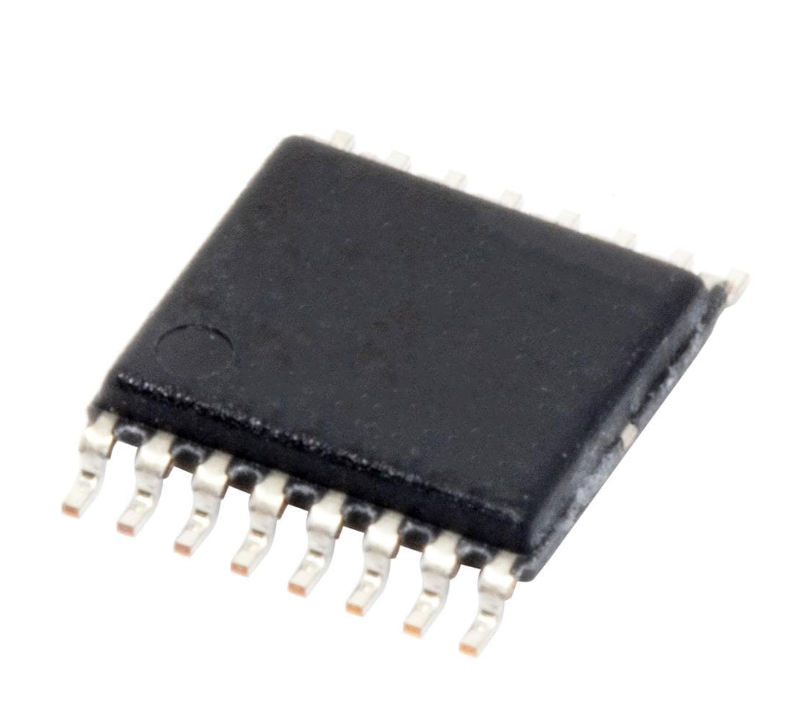
3. Ordering information
Table 1.
Ordering information
Type number
74LV4053D-Q100
Package
Temperature range
Name
Description
Version
40 C to +125 C
SO16
plastic small outline package; 16 leads; body
width 3.9 mm
SOT109-1
TSSOP16
plastic thin shrink small outline package; 16 leads; SOT403-1
body width 4.4 mm
DHVQFN16
plastic dual-in line compatible thermal enhanced
very thin quad flat package; no leads; 16
terminals; body 2.5 3.5 0.85 mm
74LV4053PW-Q100 40 C to +125 C
74LV4053BQ-Q100
40 C to +125 C
SOT763-1
4. Functional diagram
E
6
VCC
16
13 1Y1
S1 11
LOGIC
LEVEL
CONVERSION
12 1Y0
DECODER
14 1Z
1 2Y1
S2 10
LOGIC
LEVEL
CONVERSION
2 2Y0
15 2Z
3 3Y1
S3 9
LOGIC
LEVEL
CONVERSION
5 3Y0
4 3Z
8
GND
Fig 1.
7
VEE
001aak341
Functional diagram
74LV4053_Q100
Product data sheet
All information provided in this document is subject to legal disclaimers.
Rev. 1 — 25 March 2014
©
Nexperia B.V. 2017. All rights reserved
2 of 25
�74LV4053-Q100
Nexperia
Triple single-pole double-throw analog switch
6
11
S1
1Y0
12
10
S2
1Y1
13
11
9
S3
1Z
EN
#
14
14
2Y0
2
2Y1
1
10
15
15
2Z
3Y0
5
3Y1
3
3Z
4
9
MUX/DMUX
0
×
0
1
0/1
12
13
1
#
2
1
5
#
3
4
6
E
001aae125
Fig 2.
Logic symbol
001aae126
Fig 3.
IEC logic symbol
Y
VCC
VEE
VCC
VCC
VCC
VEE
from
logic
VEE
Z
001aad544
Fig 4.
Schematic diagram (one switch)
74LV4053_Q100
Product data sheet
All information provided in this document is subject to legal disclaimers.
Rev. 1 — 25 March 2014
©
Nexperia B.V. 2017. All rights reserved
3 of 25
�74LV4053-Q100
Nexperia
Triple single-pole double-throw analog switch
5. Pinning information
5.1 Pinning
��/9�����4���
�
很抱歉,暂时无法提供与“74LV4053PW-Q100J”相匹配的价格&库存,您可以联系我们找货
免费人工找货