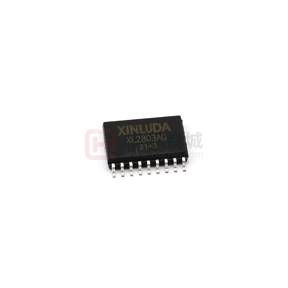
XD2803 DIP-18,XL2803AG SOP-18
8ch Darlington Sink Driver
The XD/XL2803 Series are high −voltage,
high−current darlington drivers comprised of eight NPN
darlington pairs.
All units feature integral clamp diodes for switching inductive
loads.
Applications include relay, hammer, lamp and display (LED)
drivers.
The suffix (G) appended to the part number represents a Lead
(Pb)-Free product.
Features
Type
Input Base
Resistor
Designation
2.7 k Ω
TTL, 5 V CMOS
XD/XL2803
Output current (single output)
500 mA (Max.)
High sustaining voltage output
50 V (Min.)
Pin Connection (top view)
Output clamp diodes
Inputs compatible with various types of logic.
Schematics (each driver)
XD/XL2803
Note:
The input and output parasitic diodes cannot be used as clamp diodes.
Absolute Maximum Ratings (Ta = 25°C)
Characteristic
Symbol
Rating
Unit
VCE (SUS)
−0.5~50
V
Output current
IOUT
500
mA / ch
Input voltage
VIN
−0.5~30
V
Clamp diode reverse voltage
VR
50
V
Clamp diode forward current
IF
500
mA
Output sustaining voltage
Power dissipation
XD2803
XL2803AG
PD
147
0.92 / 1.31 (Note)
W
Operating temperature
Topr
−40~85
°C
Storage temperature
Tstg
−55~150
°C
Note:
On Glass Epoxy PCB (75 × 114 × 1.6 mm Cu 20%)
1
�XD2803 DIP-18,XL2803AG SOP-18
Recommended Operating Conditions (Ta = −40~85°C)
Characteristic
Output sustaining voltage
Symbol
VCE (SUS)
XD2803
Output current
IOUT
XL2803AG
Input voltage
Input voltage
(Output on)
Clamp diode forward current
IF
Note:
XD2803
XL2803AG
PD
Typ.
Max
Unit
V
0
―
50
0
―
347
Tpw = 25 ms, Duty = 50%,
8 Circuits
0
―
123
Tpw = 25 ms, Duty = 10%,
8 Circuits
0
―
268
Tpw = 25 ms, Duty = 50%,
8 Circuits
0
―
90
VIN (ON)
VR
Min
Tpw = 25 ms, Duty = 10%,
8 Circuits
VIN
XD/XL2803
Clamp diode reverse voltage
Power dissipation
Test Condition
Ta = 85°C
Ta = 85°C
On Glass Epoxy PCB (75 × 114 × 1.6 mm Cu 20%)
2
(Note)
mA /
ch
0
―
30
3.5
―
30
V
―
―
50
V
―
―
400
mA
―
―
0.76
―
―
0.48
V
W
�XD2803 DIP-18,XL2803AG SOP-18
Electrical Characteristics (Ta = 25°C)
Characteristic
Output leakage current
Collector−emitter saturation voltage
Input current
Input voltage
(Output on)
XD/XL2803
XD/XL2803
DC current transfer ratio
Symbol
Test
Cir−
Cuit
ICEX
1
VCE (sat)
2
IIN (ON)
2
IIN (OFF)
4
VIN (ON)
hFE
5
2
Clamp diode reverse current
IR
6
Clamp diode forward voltage
VF
7
Input capacitance
CIN
―
Turn−on delay
tON
Turn−off delay
tOFF
Note:
8
Test Condition
Min
Typ.
Max
Unit
VCE = 50 V
Ta = 25°C
―
―
50
VCE = 50 V
Ta = 85°C
―
―
100
IOUT = 350 mA, IIN = 500 µA
―
1.3
1.6
IOUT = 200 mA, IIN = 350 µA
―
1.1
1.3
IOUT = 100 mA, IIN = 250 µA
―
0.9
1.1
VIN = 3.85 V
―
0.93
1.35
mA
µA
IOUT = 500 µA, Ta = 85°C
50
65
―
VCE = 2 V, IOUT = 200 mA
―
―
2.4
VCE = 2 V, IOUT = 250 mA
―
―
2.7
VCE = 2 V, IOUT = 300 mA
―
―
3.0
VCE = 2 V, IOUT = 350 mA
µA
V
V
1000
―
―
Ta = 25°C
(Note)
―
―
50
Ta = 85°C
(Note)
―
―
100
―
―
2.0
V
pF
IF = 350 mA
―
15
―
RL = 125 Ω, VOUT = 50 V
―
0.1
―
RL = 125 Ω, VOUT = 50 V
―
0.2
―
VR = VR MAX.
3
µA
µs
�XD2803 DIP-18,XL2803AG SOP-18
Test Circuit
1.
ICEX
2.
VCE (sat), hFE
3.
IIN (ON)
4.
IIN (OFF)
5.
VIN (ON)
6.
IR
7.
VF
4
�XD2803 DIP-18,XL2803AG SOP-18
8.
tON, tOFF
Note 1: Pulse Width 50 µs, Duty Cycle 10%
Output Impedance 50 Ω, tr ≤ 5 ns, tf ≤ 10 ns
Note 2: See below.
Input Condition
Type Number
XD/XL2803
R1
VIH
0Ω
3V
Note 3: CL includes probe and jig capacitance
Precautions for Using
This IC does not integrate protection circuits such as overcurrent and overvoltage protectors.
Thus, if excess current or voltage is applied to the IC, the IC may be damaged. Please design the IC so that
excess current or voltage will not be applied to the IC.
Utmost care is necessary in the design of the output line, COMMON and GND line since IC may be destroyed
due to short−circuit between outputs, air contamination fault, or fault by improper grounding.
XD/XL2803
5
�XD2803 DIP-18,XL2803AG SOP-18
XD/XL2803
6
�XD2803 DIP-18,XL2803AG SOP-18
Package Dimensions
DIP18
Unit: mm
7
�XD2803 DIP-18,XL2803AG SOP-18
Package Dimensions
Unit: mm
SOP-18
8
�
很抱歉,暂时无法提供与“XL2803AG”相匹配的价格&库存,您可以联系我们找货
免费人工找货- 国内价格
- 5+2.03138
- 50+1.64322
- 150+1.47690
- 国内价格
- 1+1.25400
- 50+0.96910
- 1000+0.89320