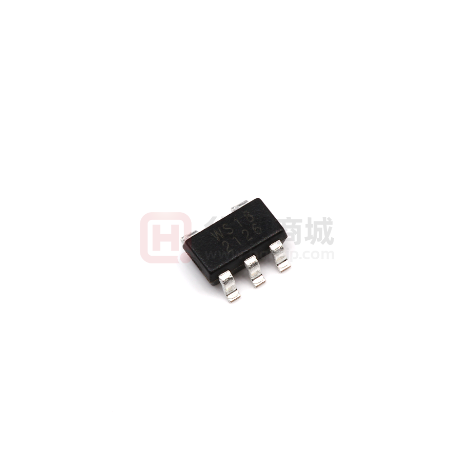
WL2803E
WL2803E
Ultra low dropout, 500mA, CMOS LDO
Http://www.sh-willsemi.com
Descriptions
The WL2803E series are ultra low dropout, Low
quiescent current, high PSRR CMOS LDO. The
dropout voltage is 130mV (Typ.) at 500mA load
current.
SOT-23-5L
Using CMOS construction, the quiescent current
consumed by the WL2803E is typically 150uA over the
entire input voltage range, making it attractive for
consumer, networking applications that demand high
output current. The WL2803E series are available in
wide output voltage range version from 1.2V to 3.3V
with 0.1V step.
The WL2803E series offer thermal shutdown (OTP)
and current limit functions, to assure the stability of
Pin Configuration (Top View)
chip and power system at wrong condition, and it uses
trimming technique to guarantee output voltage
accuracy within ±2%.
The WL2803E regulators are available in SOT-23-5L
packages.
Standard
products
are
Pb-free
and
Halogen-free.
Features
Input voltage
: 2.5V~5.5V
WS = Device code
Output voltage
: 1.2V~3.3V
**
= Voltage code (33: 3.3V)
Output current
: 500mA
YY
= Year code
PSRR
: 65dB @ 1KHz
WW = Week code
Dropout voltage
: 130mV @ IOUT=0.5A
Output noise
: 100uV
Quiescent current : 150μA Typ.
Marking
Order Information
For detail information, Please refer to page 9.
Applications
LCD TV
STB
Computer, Graphic card
Network communication equipments
Others portable electronics devices
Will Semiconductor Ltd.
1
Jul. 2019 – Rev 2.1
�WL2803E
Typical Application
VIN
4.7uF
ON
1
5
2
3
VOUT
4.7uF
Pin Description
4
OFF
PIN
Symbol
Description
1
VIN
Input
2
GND
Ground
3
EN
Enable, Active High
4
NC
Not connect
5
VOUT
Output
When the output is less than 2V, it is recommended
that the Cout is more than 10uF.
Block Diagram
Will Semiconductor Ltd.
2
Jul. 2019 – Rev 2.1
�WL2803E
Absolute Maximum Ratings
Parameter
Symbol
Input voltage range
Output voltage range
Power dissipation * *
1 3
Value
VIN
-0.3~6.5
V
VOUT
-0.3~VIN
V
0.7
W
PD
Power dissipation * *
2 3
Thermal resistance *
1
0.5
RθJA
Thermal resistance *
2
Unit
W
180
o
250
o
C/W
C/W
Junction temperature
TJ
150
o
Lead temperature(10s)
TL
260
o
Tstg
-55 ~ 150
o
HBM
±8000
V
MM
±400
V
Storage temperature
ESD Ratings
C
C
C
Note: These are stress ratings only. Stresses exceeding the range specified under “Absolute Maximum
Ratings” may cause substantial damage to the device. Functional operation of this device at other conditions
beyond those listed in the specification is not implied and prolonged exposure to extreme conditions may
affect device reliability.
*1: Surface mounted on FR-4 Board using 1 square inch pad size, dual side, 1oz copper
*2: Surface mounted on FR-4 board using minimum pad size, 1oz copper
*3: Power dissipation is calculate by PD = (VIN-VOUT) x IOUT
Recommend Operating Ratings
Parameter
Symbol
Operating Supply voltage
Operating Temperature Range
Will Semiconductor Ltd.
3
Value
Unit
VIN
2.5~5.5
Topr
-40~85
V
C
o
Jul. 2019 – Rev 2.1
�WL2803E
Electronics Characteristics (Ta=25oC, VIN=VOUT+1V, CIN=COUT=4.7uF, unless otherwise noted)
Parameter
Symbol
Condition
VOUT
很抱歉,暂时无法提供与“WL2803E18-5/TR”相匹配的价格&库存,您可以联系我们找货
免费人工找货- 国内价格
- 1+0.45650
- 200+0.29480
- 1500+0.25630
- 3000+0.22660
- 国内价格
- 1+0.55790
- 10+0.41260
- 100+0.35370
- 1000+0.29470
- 国内价格
- 10+0.67050
- 100+0.55075
- 600+0.46398
- 1200+0.45702
- 3000+0.44331
- 国内价格
- 10+0.77037
- 100+0.63278
- 300+0.53309
