SS32B THRU SS3200B
Reverse Voltage - 20 to 200 Volts
Forward Current - 3.0 Ampere
SURFACE MOUNT SCHOTTKY BARRIER RECTIFIER
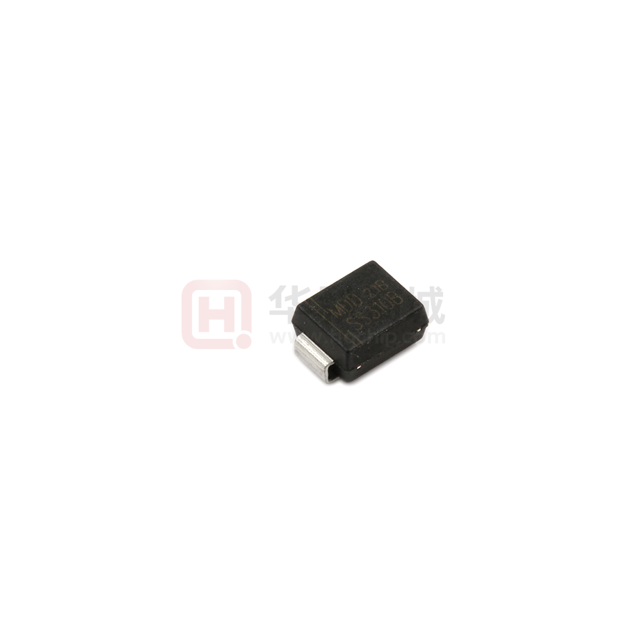
DO-214AA/SMB
Features
The plastic package carries Underwriters Laboratory
Flammability Classification 94V-0
For surface mounted applications
Metal silicon junction,majority carrier conduction
Low power loss,high efficiency
0.155(3.94)
0.130(3.30)
0.086 (2.20)
0.071 (1.80)
Built-in strain relief,ideal for automated placement
0.185(4.70)
0.160(4.06)
High forward surge current capability
High temperature soldering guaranteed:
0.012(0.305)
0.006(0.152)
250 °C/10 seconds at terminals
0.096(2.44)
0.084(2.13)
0.060(1.52)
0.030(0.76)
0.008(0.203)MAX.
Mechanical Data
0.220(5.59)
0.200(5.08)
Case�: JEDEC DO-214AA/SMB molded plastic body
Terminals�: Solderable per MIL-STD-750,Method 2026
Polarity�: Color band denotes cathode end Mounting
Position�: Any
Weight : 0.003 ounce, 0.095 grams
Dimensions in inches and (millimeters)
Maximum Ratings And Electrical Characteristics
Ratings at 25 C ambient temperature unless otherwise specified.
Single phase half-wave 60Hz,resistive or inductive load,for capacitive load current derate by 20%.
Parameter
SYMBOLS
Marking Code
Maximum repetitive peak reverse voltage
Maximum RMS voltage
Maximum DC blocking voltage
VRRM
VRMS
VDC
MDD
SS32B
MDD
SS33B
MDD
SS34B
MDD
SS35B
MDD
SS36B
MDD
SS38B
MDD
SS310B
MDD
SS3150B
MDD
SS3200B
UNITS
20
14
20
30
21
30
40
28
40
50
35
50
60
42
60
80
56
80
100
70
100
150
105
150
200
140
200
V
V
V
Maximum average forward rectified current
I(AV)
3
A
Peak forward surge current
8.3ms single half sine-wave
superimposed onrated load (JEDEC Method)
IFSM
80
A
Maximum instantaneous forward voltage at 3.0A
VF
Maximum DC reverse current
at rated DCblocking voltage
TA=25℃
TA=100℃
Typical junction capacitance (NOTE 1)
0.55
IR
CJ
0.5
0.7
0.85
5
450
400
V
0.95
0.3
3
mA
pF
Typical thermal resistance (NOTE 2)
RJA
60
℃/W
Operating junction temperature range
TJ
-55 to +150
℃
TSTG
-55 to +150
℃
Storage temperature range
Note:1.Measured at 1MHz and applied reverse voltage of 4.0V D.C.
2.P.C.B. mounted with 2.0”x2.0”(5.0x5.0cm) copper pad areas
http://www.microdiode.com
Rev:2024A2
Page :1
�SS32B THRU SS3200B
Reverse Voltage - 20 to 200 Volts
Forward Current - 3.0 Ampere
Typical Characterisitics
Fig.2 Typical Reverse Characteristics
3.5
3.0
2.4
1.8
1.2
0.6
0.0
25
50
75
100
125
150
Instaneous Reverse Current ( μA)
Average Forward Current (A)
Fig.1 Forward Current Derating Curve
10
4
10
3
10
2
TJ=100°C
TJ=75°C
SS32B/SS36B
TJ=25°C
0
10
0
Case Temperature (°C)
40
60
80
100
Fig.4 Typical Junction Capacitance
TJ=25°C
20
1000
10
1.0
Junction Capacitance (pF)
500
SS32B/SS34B
SS36B
SS38B/SS312B
SS315B/SS3200B
0.1
0
0.2
0.4
0.6
0.8
1.0
1.2
1.4
1.6
1.8
200
100
20
SS32B~SS36B
SS38B~SS3200B
10
0.1
Fig.5 Maximum Non-Repetitive Peak
Forward Surage Current
10
100
Fig.6- Typical Transient Thermal Impedance
100
60
40
20
8.3 ms Single Half Sine Wave (JEDEC
Method)
1
10
Number of Cycles at 60Hz
100
Transient Thermal Impedance(°C/W)
100
80
00
1
Reverse Voltage (V)
Instaneous Forward Voltage (V)
Peak Forward Surage Current (A)
20
Percent of Rated Peak Reverse Voltage(%)
Fig.3 Typical Forward Characteristic
Instaneous Forward Current (A)
SS38B~SS3200B
101
10
1
0.01
0.1
1
10
100
t, Pulse Duration(sec)
The curve above is for reference only.
http://www.microdiode.com
Rev:2024A2
Page :2
�SS32B THRU SS3200B
Reverse Voltage - 20 to 200 Volts
Forward Current - 3.0 Ampere
Packing information
unit:mm
P0
P1
Item
Symbol
Tolerance
SMB
Carrier width
Carrier length
Carrier depth
Sprocket hole
13" Reel outside diameter
13" Reel inner diameter
Feed hole diameter
Sprocket hole position
Punch hole position
Punch hole pitch
Sprocket hole pitch
Embossment center
Overall tape thickness
Tape width
A
B
C
d
D
D1
D2
E
F
P
P0
P1
T
W
Reel width
W1
0.1
0.1
0.1
0.05
2.0
min
0.5
0.1
0.1
0.1
0.1
0.1
0.1
0.3
1.0
3.81
5.41
2.42
1 50
.
330.00
50.00
13.00
1.75
5.55
8.00
4.00
2.00
0.30
12.00
12.30
d
E
F
B
A
W
P
D2
T
D1
C
W1
D
Note:Devices are packed in accor dance with EIA standar RS-481-A and specifications listed above.
Reel packing
PACKAGE
REEL SIZE
REEL
(pcs)
COMPONENT
SPACING
(mm)
BOX
(pcs)
INNER
BOX
(mm)
REEL
DIA,
(mm)
SMB
13"
3,000
4.0
6,000
190*190*41
330
CARTON
SIZE
(mm)
365*365*360
CARTON
(pcs)
48,000
APPROX.
GROSS WEIGHT
(kg)
14.0
Suggested Pad Layout
http://www.microdiode.com
Unit (inch)
Symbol
Unit (mm)
A
2.8
0.110
B
0.094
C
2.4
4.6
0.181
D
2.2
0.086
E
7.0
0.276
Rev:2024A2
Page :3
�
很抱歉,暂时无法提供与“SS310B”相匹配的价格&库存,您可以联系我们找货
免费人工找货- 国内价格
- 10+0.26685
- 100+0.21779
- 600+0.19334
- 1200+0.19044
- 国内价格
- 1+0.25740
- 200+0.16500
- 1500+0.14410
- 3000+0.12760
- 国内价格
- 10+0.30338
- 100+0.24759
- 300+0.21981
- 3000+0.16537
- 6000+0.14868
- 9000+0.14029