富满微电子集团股份有限公司
FINE MADE MICROELECTRONICS GROUP CO., LTD.
FM8544A (文件编号:S&CIC2065)
SP4T Switch for 4G/5G Applications
Features
Description
Broadband frequency range: 0.1 to 3.0GHz
Low insertion loss: 0.70dB @2.7GHz
The FM8544A is a CMOS silicon-on-insulator (SOI),
High P0.1dB of 43dBm
single- pole, four-throw (SP4T) switch. The high linearity
Off Ports, “Open Type”
and ruggedness performance and extremely low
Three pin GPIO control Interface for multi-on application
insertion loss makes the device an ideal choice for
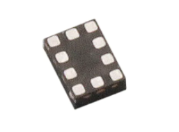
Small QFN (10-pin, 1.1mm x 1.5mm x 0.45mm) package,
GSM/WCDMA/LTE handset antenna tuning application.
MSL1
The FM8544A SP4T switch is provided in a compact
QFN 1.1mm x 1.5mm x 0.45mm package. A functional
block diagram is shown in Figure 1. The pin
Applications
configuration and package are shown in Figure 2. Signal
GSM/WCDMA/LTE band and mode switching
pin assignments and functional pin descriptions are
Antenna tuning switch
provided in Table 1.
Figure 1 Functional Block Diagram
Figure 2 Pin-Out(Top View)
Version 1.0
Page 1
Copyright©2021, ShenZhen FM Co.ltd
�富满微电子集团股份有限公司
FINE MADE MICROELECTRONICS GROUP CO., LTD.
FM8544A (文件编号:S&CIC2065)
SP4T Switch for 4G/5G Applications
Function Characteristics
Figure 3 Application Circuit
Table 1 Pin Description
No.
Name
Description
No.
Name
Description
1
RF1
RF Port 1
6
V2
Logic Control Voltage 2
2
RF2
RF Port 2
7
GND
Ground
3
V3
Logic Control Voltage 3
8
RF4
RF Port 4
4
VDD
DC Power Supply
9
RF3
RF Port 3
5
V1
Logic Control Voltage 1
10
ANT
Antenna Port
Table 2 VC Truth Table of for RF Channel Operating Mode
RF Channel Operating
V1
V2
V3
Low
Low
High
All Ron
Low
High
High
ANT to RF1 and RF2
Version 1.0
Page 2
Mode
Copyright©2021, ShenZhen FM Co.ltd
�富满微电子集团股份有限公司
FINE MADE MICROELECTRONICS GROUP CO., LTD.
FM8544A (文件编号:S&CIC2065)
SP4T Switch for 4G/5G Applications
High
Low
High
ANT to RF3 and RF4
Low
Low
Low
ANT to RF1
Low
High
Low
ANT to RF2
High
Low
Low
ANT to RF3
High
High
Low
ANT to RF4
High
High
High
All isolation
Electrical Characteristics
Table 3 Absolute Maximum Ratings
Parameter
Symbol
Min
Max
Unit
VDD
-0.3
+4.8
V
VC
-0.3
+3.3
V
PIN
+43
dBm
Vpeak
60
V
DC Supply Voltage
Digital Control Voltage
RF Input Peak Power
Max Input Power between any combination of RF
ports or ground VRF,
VDD = 2.85VDC, VCTL1/2 = 0/1.8VDC, Temp =
25℃ @20% DC
Max voltage between any combination of RF
ports or ground VRF,
VDD = 2.85VDC, VCTL1/2 = 0/1.8VDC, Temp =
25℃ @20% DC
Device Operating Temperature
TOP
-40
+90
℃
Device Storage Temperature
TSTG
-55
+150
℃
Electrostatic Discharge
Human Body Model (HBM), Class 2
VESD(HBM)
Charged Device Model (CDM), Class III
VESD(CDM)
1000
1000
V
V
Notice
Exposure to maximum rating conditions for extended periods may reduce device reliability. There is no damage to device with
only one parameter set at the limit and all other parameters set at or below their nominal value. Exceeding any of the limits listed
here may result in permanent damage to the device.
Version 1.0
Page 3
Copyright©2021, ShenZhen FM Co.ltd
�富满微电子集团股份有限公司
FINE MADE MICROELECTRONICS GROUP CO., LTD.
FM8544A (文件编号:S&CIC2065)
SP4T Switch for 4G/5G Applications
Table 4 Recommended Operating Conditions
Parameter
Symbol
MIN
F0
0.1
DC Supply Voltage
VDD
2.5
Logic Control Voltage High
VCH
Logic Control Voltage Low
VCL
Operating Frequency
TYP
MAX
Unit
3.0
GHz
2.8
4.2
V
1.0
1.8
3.0
V
0
0
0.3
V
Table 5 Nominal Operating Parameters
Parameter
Symbol
Specification
MIN
Normal Condition
TYP
Unit
Condition
MAX
VDD=2.8V, VCH=1.8V, VCL=0V, PIN=0dBm, ZO=50Ω, TA=25℃, Unless Otherwise
Stated
DC Performances
DC Supply Current
Current on Logic Control
IDD
80
IC
120
μA
1
5
μA
Startup Time
TON
10
20
μs
Switching Speed
TSW
4
5
μs
50% of final VDD to 90% of the final RF
50% of final VC to 90%/10% of the final
RF
RF Performances
Insertion Loss
IL
(ANT to RF1/2/3/4)
Isolation
(ANT to RF1/2/3/4)
ISO
0.30
0.35
0.50
0.60
0.70
0.85
21
23
17
20
12
14
dB
dB
dB
dB
dB
dB
F0=0.8 to 1.0GHz
F0=1.0 to 2.2GHz
F0=2.2 to 3.0GHz
F0=0.8 to 1.0GHz
F0=1.0 to 2.2GHz
F0=2.2 to 3.0GHz
Return Loss
(ANT to RF1/2/3/4)
RL
15
dB
RON
1.0
1.5
COF
150
170
F0=0.8 to 3.0GHz
On Resistance
(ANT to RF1/2/3/4)
Switch On Path@DC
Off Capacitance
(ANT to RF1/2/3/4)
Version 1.0
fF
Switch Off Path@500MH
F
Page 4
Copyright©2021, ShenZhen FM Co.ltd
�富满微电子集团股份有限公司
FINE MADE MICROELECTRONICS GROUP CO., LTD.
FM8544A (文件编号:S&CIC2065)
SP4T Switch for 4G/5G Applications
Peak RF Operating
VRF
60
LTE TX Harmonic
2F0
-70
-65
dBm
(RF1/2/3/4 to ANT)
3F0
-75
-65
dBm
GSM LB Harmonic
2F0
-60
-52
dBm
(RF1/2/3/4 to ANT)
3F0
-70
-60
dBm
GSM HB Harmonic
2F0
-65
-58
dBm
(RF1/2/3/4 to ANT)
3F0
-70
-60
dBm
Voltage
V
F0=950MHz, 20% duty cycle
F0= 0.7 to 2.7GHz @+26dBm
F0= 824 to 915MHz @+35dBm
F0= 1710 to 2690MHz @+33dBm
Tape and Reel Dimensions
Figure 6 Tape and Reel Dimensions
Version 1.0
Page 5
Copyright©2021, ShenZhen FM Co.ltd
�富满微电子集团股份有限公司
FINE MADE MICROELECTRONICS GROUP CO., LTD.
FM8544A (文件编号:S&CIC2065)
SP4T Switch for 4G/5G Applications
Reflow Chart
Figure 7 Recommended Lead-Free Reflow Profile
Table 7 Reflow Chart Parameters
Reflow Profile
Parameter
Preheat Temperature(TSMIN to TSMAX)
150℃ to 200℃
60 to 180 Seconds
Preheat Time(ts)
Ramp-Up Rate(TSMAX to TP)
3℃/s MAX
60 to 150 Seconds
Time Above TL 217℃(tL)
Peak Temperature(TP)
260℃
Time within 5℃ of Peak Temperature(tP)
20 to 40 Seconds
Ramp-Down Rate(TSMAX to TP)
6℃/s MAX
Time for 25℃ to Peak Temperature(t25-TP)
8 Minutes MAX
ESD Sensitivity
Integrated circuits are ESD sensitive and can be damaged by static electric charge. Proper ESD protection techniques should be
applied when devices are operating.
RoHS Compliant
This product does not contain lead, mercury, cadmium, hexavalent chromium, polybrominated biphenyls (PBB) and
polybrominated diphenyl ethers (PBDE), and is considered RoHS compliant.
Version 1.0
Page 6
Copyright©2021, ShenZhen FM Co.ltd
�
很抱歉,暂时无法提供与“FM8544A”相匹配的价格&库存,您可以联系我们找货
免费人工找货- 国内价格
- 5+1.25499
- 50+1.00058
- 1000+0.75558
- 2000+0.69502
- 5000+0.68112