山东晶导微电子股份有限公司
D2N65
Jingdao Microelectronics co.LTD
2A, 650V N-CHANNEL
POWER MOSFET
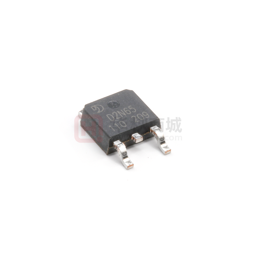
TO-252W
DESCRIPTION
The D2N65 is a high voltage power MOSFET combines
advanced trench MOSFET designed to have better characteristics,
such as fast switching time, low gate charge, low on-state
resistance and high rugged avalanche characteristics. This power
MOSFET is usually used in high speed switching applications of
switching power supplies and adaptors.
PIN1
PIN2
PIN3
Features
• RDS(ON) ≤4.3 Ω @ VGS=10V, ID=2.0A
• Fast switching capability
• Avalanche energy tested
• Improved dv/dt capability, high ruggedness
SYMBOL
2.4.Drain
Mechanical data
• Case: TO-252W
• A pprox. Weight: 0.315g ( 0.011oz)
• Lead free finish, RoHS compliant
• Case Material: “Green” molding compound, UL
flammability classification 94V-0,“Halogen-free”.
1.Gate
3.Source
ABSOLUTE MAXIMUM RATINGS (TA=25°C, unless otherwise specified)
Symbols
RATINGS
Drain-Source Voltage
V DSS
650
V
Gate-Source Voltage
V GSS
±30
V
Continuous Drain Current
ID
2
A
Pulsed Drain Current (Note 2)
I DM
8
A
Avalanche Energy
E AS
108
mJ
dv/dt
2.1
V/ns
PD
32
W
T j, T stg
-55 ~ +150
°C
PARAMETER
Single Pulsed (Note 3)
Peak Diode Recovery dv/dt (Note 4)
Power Dissipation
Operation Junction Temperature and
Storage Temperature
Units
Notes: 1. Absolute maximum ratings are those values beyond which the device could be permanently damaged.
Absolute maximum ratings are stress ratings only and functional device operation is not implied.
2. Repetitive Rating: Pulse width limited by maximum junction temperature.
3. L = 30mH, IAS = 3.4A, VDD = 50V, RG = 25 Ω, Starting TJ = 25°C
4. ISD ≤ 2A, di/dt ≤200A/μs, VDD ≤ BVDSS, Starting TJ = 25°C
THERMAL DATA
PARAMETER
Symbols
RATINGS
Units
Junction to Ambient
R thJA
63
°C/W
Junction to Case
R thJC
2.31
°C/W
Note: Device mounted on FR-4 substrate PC board, 2oz copper, with 1inch square copper plate.
2021.06
TO-252W-MOS-D2N65-2A650V
Page 1 of 8
�山东晶导微电子股份有限公司
D2N65
Jingdao Microelectronics co.LTD
ELECTRICAL CHARACTERISTICS (TA=25°C, unless otherwise specified)
Symbols
PARAMETER
TEST CONDITIONS
Min
Typ
Max
Units
OFF CHARACTERISTICS
Drain-Source Breakdown Voltage
Drain-Source Leakage Current
BV DSS
VDS=0V,ID=250uA
I DSS
VDS=650V,VGS=0V
1
VGS=30V,VDS=0V
100
VGS=-30V,VDS=0V
-100
Forward
I GSS
Gate- Source Leakage Current
Reverse
650
V
uA
nA
ON CHARACTERISTICS
Gate Threshold Voltage
VGS(TH)
VDS=VGS,ID=250uA
Static Drain-Source On-State Resistance
RDS(ON)
VGS=10V,ID=2.0A
4.3
2.0
4.0
V
5
Ω
DYNAMIC CHARACTERISTICS
Input Capacitance
CISS
VDS=25V,
260
pF
Output Capacitance
COSS
VGS=0V,
30
pF
Reverse Transfer Capacitance
CRSS
f=1.0MHz
2.2
pF
QG
VDS=520V,VGS=10V,
8.97
nC
Gate-Source Charge
QGS
ID=2A,IG=1mA
2.51
nC
Gate-Drain Charge
QGD
(NOTE1,2)
4.02
nC
tD(ON)
VDS=325V,VGS=10V,
8.4
ns
ID=2A,RG=25Ω
22.4
ns
(NOTE1,2)
15.1
ns
24.1
ns
SWITCHING CHARACTERISTICS
Total Gate Charge (Note 1)
Turn-On Delay Time (Note 1)
Turn-On Rise Time
tR
Turn-Off Delay Time
tD(OFF)
Turn-Off Fall Time
tF
DRAIN-SOURCE DIODE CHARACTERISTICS AND MAXIMUM RATINGS
IS
2
A
Maximum Body-Diode Pulsed Current
ISM
8
A
Drain-Source Diode Forward Voltage (Note 1)
VSD
IS=2A,VGS=0V
1.4
V
trr
IS=2A,VGS=0V,
370
ns
Qrr
di/dt=100A/us
0.95
uC
Maximum Body-Diode Continuous Current
Reverse Recovery Time (Note 1)
Reverse Recovery Charge
Notes:
1. Pulse Test: Pulse width ≤ 300μs, Duty cycle ≤ 2%.
2. Essentially independent of operating temperature.
2021.06
www.sdjingdao.com
Page 2 of 8
�山东晶导微电子股份有限公司
D2N65
Jingdao Microelectronics co.LTD
Test Circuits and waveforms
+
D.U.T
VDS
+
ISD
-
RG
VGS
Driver
VDD
*dv/dt controlled by RG
* ISD controlled by pulse period
* D.U.T.-Device Under Test
Same Type
as D.U.T
Peak Diode Recovery dv/dt Test Circuit
Period
VGS
(Driver)
D=
P.W
P.W
Period
VGS=10V
IFM,Body Diode Forward Current
di/dt
ISD
(D.U.T)
IRM
Body Diode Reverse Current
Body Diode Reverse Current
VDS
(D.U.T)
VDD
Body Diode
Forward Voltage Drop
Peak Diode Recovery dv/dt Waveforms
2021.06
www.sdjingdao.com
Page 3 of 8
�山东晶导微电子股份有限公司
D2N65
Jingdao Microelectronics co.LTD
Test Circuits and waveforms
RL
VDS
VDS
90%
VGS
RG
VDD
10%
VGS
Pulse Width≤ 1μs
Duty Factor≤0.1%
D.U.T
tD(ON)
Switching Test Circuit
tD(OFF)
tR
tF
Switching Waveforms
VGS
QG
Same Type
as D.U.T
QGS
QGD
VDS
VGS
D.U.T
Charge
Gate Charge Test Circuit
Gate Charge Waveform
L
VDS
BVDSS
IAS
RD
ID(t)
VDD
tP
VDS(t)
VDD
D.U.T
tP
Unclamped Inductive Switching Test Circuit
2021.06
Time
Unclamped Inductive Switching Waveforms
www.sdjingdao.com
Page 4 of 8
�山东晶导微电子股份有限公司
D2N65
Jingdao Microelectronics co.LTD
Typical Characteristics
Fig.1 Drain Current vs. Gate-Source Voltage
Fig.2 Drain-Source On-Resistance vs. Gate-Source Voltage
6
Drain-Source On-Resistance, RDS(ON) (Ω)
6
TA=25°C
Pulsed test
VGS=6~10V
Drain Current, ID (A)
5
4
VGS=6V
3
VGS=5.5V
2
VGS=5V
1
VGS=4.5V
0
0
4
8
12
16
20
24
TA=25°C
Pulsed test
5
4
3
ID=2.0A
2
ID=1.0A
1
0
28
0
2
Drain-Source Voltage, VDS (V)
6
4
8
10
12
14
Gate-Source Voltage, VGS (V)
Fig.3 Gate Charge Characteristics
Fig.4 Capacitance Characteristics
10
VDS=520V VGS=10V ID=2A Pulsed
500
COSS
8.0
Capacitance, C (pF)
Gate-Source Voltage, VGS (V)
600
6.0
4.0
400
CISS
300
200
CRSS
2.0
100
0.0
2
4
6
8
10
12
14
0
10
Total Gate Charge, QG (nC)
Fig.6 Breakdown Voltage vs. Junction Temperature
1.2
Drain-Source Breakdown Voltage Normalized
3.0
Drain-Source On-Resistance Normalized
1000
Drain-Source Voltage, VDS (V)
Fig.5 Drain-Source On-Resistance vs. Junction Temperature
2.5
100
VGS=10V
ID=1.0A
Pulsed
2.0
1.5
1.0
0.5
0
25
50
75
100
125
150
ID=0.25mA Pulsed
1.0
0.8
0.6
0.4
0.2
0
25
175
Junction Temperature, TJ (°C)
75
50
100
125
150
175
Junction Temperature, TJ (°C)
Fig.8 Source Current vs. Source-Drain Voltage
Fig.7 Gate Threshold Voltage vs. Junction Temperature
10
0.5
0.25
15
A=
25
°C
A=
1.0
T
0.75
T
1.0
0
°C
1.25
Source Current, IS (A)
Gate Threshold Voltage Normalized
ID=0.25mA Pulsed
0.1
0
25
50
75
100
125
150
175
0.2
0.4
0.6
0.8
1.0
1.2
1.4
Source-Drain Voltage, VSD (V)
Junction Temperature, TJ (°C)
2021.06
0
www.sdjingdao.com
Page 5 of 8
�山东晶导微电子股份有限公司
D2N65
Jingdao Microelectronics co.LTD
Typical Characteristics
Fig.10 Drain-Source On-Resistance vs. Drain Current
Fig.9 Drain Current vs. Gate-Source Voltage
TA=25°C Pulsed
5
Drain Current, ID (A)
Drain-Source On-Resistance, RDS(ON) (Ω)
8.0
4
3
2
1
0
1
3
2
4
5
6
7.0
TA=25°C
VGS=10V
Pulsed
6.0
5.0
4.0
3.0
2.0
1.0
0
1
2
7
3
5
4
Drain Current, ID (A)
Junction Temperature, TJ (°C)
Fig.12 Power Dissipation vs. Junction Temperature
Fig.11 Drain Current vs. Junction Temperature
2.5
Power Dissipation, PD (W)
Drain Current, ID (A)
50
2.0
1.5
1.0
0.5
40
30
20
10
RESISTIVE OR INDUCTIVE LOAD
0
0.0
25
75
50
100
125
150
175
Junction Temperature, TJ (°C)
25
50
75
100
125
150
175
Junction Temperature, TJ (°C)
Fig.13 Safe Operating Area
10
Max
100us
Drain Current, I (A)
1ms
1.0
10ms
Operation in this area
is limited by RDS(ON)
0.1
DC
TJ=150°C
TC=25°C Single Pulse
0.01
1.0
10
100
1000
Drain-Source Voltage, VDS (V)
2021.06
www.sdjingdao.com
Page 6 of 8
�山东晶导微电子股份有限公司
D2N65
Jingdao Microelectronics co.LTD
TO-252W(D-PAK) Package Outline Dimensions
A
B
C
E
L1
+
D
M
NN
J
K
T
S
L2
L
b
G
L3
H
G
F
TO-252W(D-PAK) mechanical data
UNIT
A
max 6.7
B
b
C
D
E
F
5.5
0.8
2.5
6.3
0.6
1.8
G
H
L
L1
L2
0.55 3.1
1.2
1.0 1.75 0.1
1.0
3.16 1.80 4.83
1.8
1.3
0.8 1.30 0.08 TYPICAL TYPICAL ref. ref. ref.
0.8
0.6 1.00 0.0
6.6
5.3
0.7
2.3
6.1
0.5
min 6.3
5.1
0.3
2.1
5.9
0.4
2.29
0.50 2.8
1.5
TYPICAL
1.3
0.45 2.7
max 264 217
31
98
248
24
71
mil typ 260 209
28
90
240
20
59
min 248 201
12
83
232
16
51
mm
typ
90
TYPICAL
L3
S
22
122
47
39
69
4
20
110
39
31
51
3
18
106
31
24
55
0
M
N
71
51
TYPICAL TYPICAL
J
124
ref.
K
71
ref.
T
190
ref.
MARKING DIAGRAM
Unmarkable Surfacea
C
A
B
Marking Composition Field
A: Marking Area
B: Lot Code
C: Additional Information
D
D:Date Code (YWW)
Y:Years(0~9)
WW: Week
2021.06
JD210617
Page 7 of 8
�山东晶导微电子股份有限公司
Jingdao Microelectronics co.LTD
D2N65
Important Notice and Disclaimer
Jingdao Microelectronics reserves the right to make changes to this document and
its products and specifications at any time without notice.
Customers should obtain and confirm the latest product information and specifications
before final design, purchase or use.
Jingdao Microelectronics makes no warranty, representation or guarantee regarding the
suitability of its products for any particular purpose, not does Jingdao Microelectronics
assume any liability for application assistance or customer product design.
Jingdao Microelectronics does not warrant or accept any liability with products which
are purchased or used for any unintended or unauthorized application.
No license is granted by implication or otherwise under any intellectual
property rights of Jingdao Microelectronics.
Jingdao Microelectronics products are not authorized for use as critical components
in life support devices or systems without express written approval of Jingdao Microelectronics.
2021.06
www.sdjingdao.com
Page 8 of 8
�