MOSFET
SI2309S
P-Channel Enhancement-Mode MOSFET
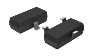
SOT-23
-
ROHS
Features
• Low RDS(on) @VGS=-10V
• -5V Logic Level Control
• P Channel SOT23 Package
• Pb−Free, RoHS Compliant
V(BR)DSS
RDS(ON) Typ
170mΩ @ 10V
-60V
Applications
ID Max
• Load Switch
• Switching Circuits
-1.9A
200mΩ @ 4.5V
• High Speed line Driver
Order Information
Product
Package
Marking
Packing
Min Unit Quantity
SI2309S
SOT23
WMGCF
3000PCS/Reel
3000PCS
Absolute Maximum Ratings
Stresses exceeding Maximum Ratings may damage the device. Maximum Ratings are stress ratings only. Functional operation above
the Recommended Operating Conditions is not implied. Extended exposure to stresses above the Recommended Operating Conditions
may affect device reliability.
Symbol
Parameter
Rating
Unit
Common Ratings (TA=25°C Unless Otherwise Noted)
VGS
Gate-Source Voltage
±20
V
V(BR)DSS
Drain-Source Breakdown Voltage
-60
V
TJ
Maximum Junction Temperature
150
°C
TSTG
Storage Temperature Range
-50 to 150
°C
TA =25°C
-7.6
A
TA =25°C
-1.9
TA =70°C
-1.5
TA =25°C
1.4
TA =70°C
0.9
Mounted on Large Heat Sink
IDM
Pulse Drain Current Tested①
ID
Continuous Drain Current
PD
Maximum Power Dissipation
R JA
Thermal Resistance Junction-Ambient
Rev 8: Nov 2018
www.born-tw.com
A
W
90
°C/W
Page 1 of 4
�MOSFET
Symbol
SI2309S
P-Channel Enhancement-Mode MOSFET
Parameter
Condition
ROHS
Min
Typ
Max
Unit
Static Electrical Characteristics @ TJ = 25°C (unless otherwise stated)
V(BR)DSS
Drain-Source Breakdown Voltage
VGS=0V ID=-250μA
-60
--
--
V
Zero Gate Voltage Drain Current(TA=25℃)
VDS=-60V, VGS=0V
--
--
-10
μA
Zero Gate Voltage Drain Current(TA=125℃)
VDS=-60V, VGS=0V
--
--
-100
uA
IGSS
Gate-Body Leakage Current
VGS=±20V, VDS=0V
--
--
±1 00
nA
VGS(TH)
Gate Threshold Voltage
VDS=VGS, ID=-250μA
-1.0
-3
V
RDS(ON)
Drain-Source On-State Resistance②
VGS=-10V, ID=-1.8A
--
170
215
mΩ
RDS(ON)
Drain-Source On-State Resistance②
VGS=-4.5V, ID=-1.4A
--
200
260
mΩ
--
364
--
pF
--
41
--
pF
--
12
--
pF
--
6.3
--
nC
--
2.3
--
nC
--
1.8
--
nC
--
20
--
ns
--
33.1
--
ns
-
5.2
--
ns
--
3.8
--
ns
-1.2
V
IDSS
Dynamic Electrical Characteristics @ T J = 25°C (unless otherwise stated)
Ciss
Input Capacitance
Coss
Output Capacitance
Crss
Reverse Transfer Capacitance
Qg
Total Gate Charge
Qgs
Gate Source Charge
Qgd
Gate Drain Charge
VDS=-25V, VGS=0V,
f=1MHz
VDS=-48V
ID=-1A,
VGS=-4.5V
Switching Characteristics
t d(on)
Turn on Delay Time
tr
Turn on Rise Time
t d(off)
Turn Off Delay Time
tf
Turn Off Fall Time
VDD=-30V,
ID=-1A,
RG=3.3Ω,
VGS=-10V
RL=30Ω
Source Drain Diode Characteristics
VSD
Tj=25℃, ISD=-1.2A,
Forward on voltage②
VGS=0V
--
Notes:
① Pulse width limited by maximum allowable junction temperature
②Pulse test ; Pulse width300s, duty cycle2%.
Rev 8: Nov 2018
www.born-tw.com
Page 2 of 4
�MOSFET
P-Channel Enhancement-Mode MOSFET
SI2309S
ROHS
P-Channel Enhancement Mode Mosfet
Typical Characteristics (TJ =25℃ Noted)
Tc, Case Temperature (°C)
Rev 8: Nov 2018
www.born-tw.com
Page 3 of 4
�MOSFET
P-Channel Enhancement-Mode MOSFET
P-Channel Enhancement Mode Mosfet
Typical Characteristics (TJ =25℃ Noted)
SI2309S
ROHS
�MOSFET
SI2309S
P-Channel Enhancement-Mode MOSFET
ROHS
SOT-23 PACKAGE OUTLINE Plastic surface mounted package
SOT-23
(UNIT):mm
Rev 8: Nov 2018
www.born-tw.com
Page 4 of 4
�
很抱歉,暂时无法提供与“SI2309S”相匹配的价格&库存,您可以联系我们找货
免费人工找货- 国内价格
- 10+0.28174
- 100+0.24960
- 300+0.23346
- 3000+0.19811
- 6000+0.18838
- 9000+0.18360
- 国内价格
- 1+0.39820
- 200+0.25630
- 1500+0.22220
- 3000+0.19800