SI2301
SOT-23 Plastic-Encapsulate MOSFETS
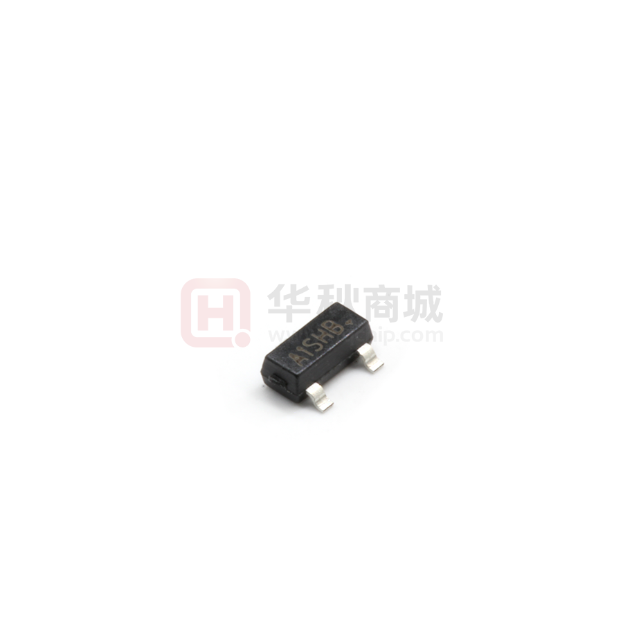
SOT-23
20V P-Channel MOSFET
V(BR)DSS
-20V
RDS(on)Typ
ID Max
70mΩ@4.5V
-3.0A
78mΩ@3.3V
3
1. GATE
2. SOURCE
1
3. DRAIN
2
APPLICATION
Load Switch for Portable Devices
z
DC/DC Converter
z
Features
Trench FET Power MOSFET
MARKING
Equivalent circuit
D
A1sHB
G
S
PACKAGE SPECIFICATIONS
Package Reel Size
SOT-23
Reel DIA.
(mm)
Q'TY/Reel
(pcs)
Box Size
(mm)
QTY/Box
(pcs)
330
3000
203×203×195
45000
7'
Carton Size Q'TY/Carton
(mm)
(pcs)
438×438×220
180000
Maximum Ratings and Thermal Characteristics (TA = 25°C unless otherwise noted)
Parameter
Symbol
Limit
Drain-Source Voltage
VDS
-20
Gate-Source Voltage
VGS
±10
TA = 25 oC
T = 70oC
Continuous Drain Current
Maximum Power Dissipation
TA = 25 C
T = 70oC
2)
Junction-to-Ambient Thermal Resistance (PCB mounted)
2)
A
-12
1.2
PD
W
0.9
A
Operating Junction and Storage Temperature Range
A
-2.5
IDM
o
V
-3.0
ID
A
Pulsed Drain Current 1)
Unit
TJ, Tstg
-50 to 150
RthJA
100
o
C
o
C/W
Notes
1) Pulse width limited by maximum junction temperature.
2) Surface Mounted on FR4 Board, t v 5 sec.
The above data are for reference only.
DN:T19928A0
http://www.microdiode.com
Rev:2019A0
Page :1
�SI2301
MOSFET ELECTRICAL CHARACTERISTICS
Ta =25 ℃ unless otherwise specified
Parameter
Symbol
Test Condition
Min
Typ
Max
-0.6
-1
Units
Static
Drain-source breakdown voltage
V(BR)DSS
VGS = 0V, ID =-250µA
-20
Gate-source threshold voltage
VGS(th)
VDS =VGS, ID =-250µA
-0.4
Gate-source leakage
IGSS
VDS =0V, VGS =±10V
±100
nA
Zero gate voltage drain current
IDSS
VDS =-20V, VGS =0V
-1
µA
Drain-source on-state resistance
Forward transconductance
a
a
RDS(on)
gfs
VGS =-4.5V, ID =-3A
70
90
VGS =-3.3V, ID =-2.0A
78
100
VDS =-5V, ID =-2.8A
4.0
V
mΩ
S
b
Dynamic
Input capacitance
Ciss
Output capacitance
Coss
Reverse transfer capacitance
Crss
Total gate charge
Qg
Gate-source charge
Qgs
Gate-drain charge
Qgd
Turn-on delay time
td(on)
Rise time
Turn-off delay time
Fall time
tr
td(off)
tf
330
VDS =-10V,VGS =0V,f =1MHz
pF
50
45
VDS =-10V,VGS =-4.5V,ID =-3A
6.6
0.8
nC
0.7
VDS =-10V,VGS =-4.5V,ID =-3A
1.4
11
VDD=-10V, RL=10Ω,
12
ID =-3A,
ns
18
VGEN=-4.5V,Rg=3.3Ω
30
Drain-source body diode characteristics
Continuous source-drain diode current
Body diode voltage
a)
b)
IS
VSD
TC=25℃
IS=-2A
-0.85
-1.5
A
-1.2
V
Pulse test: pulse width ≤ 300us, duty cycle≤ 2%
Guaranteed by design, not subject to production testing
http://www.microdiode.com
Rev:2019A0
Page :2
�SI2301
-ID, Drain-Source Current (A)
-VGS(TH), Gate -Source Voltage (V)
Typical Characteristics
-VDS, Drain -Source Voltage (V)
Fig2. Normalized Threshold Voltage Vs. Temperature
-ID, Drain-Source Current (A)
-VDS, Drain -Source Voltage (mV)
Fig1. Typical Output Characteristics
Tj - Junction Temperature (°C)
-VGS, Gate -Source Voltage (V)
Fig4. Drain -Source Voltage vs Gate -Source Voltage
-ID - Drain Current (A)
-ISD, Reverse Drain Current (A)
Fig3. Typical Transfer Characteristics
-VGS, Gate -Source Voltage (V)
-VSD, Source-Drain Voltage (V)
Fig5. Typical Source-Drain Diode Forward Voltage
http://www.microdiode.com
-VDS, Drain -Source Voltage (V)
Fig6. Maximum Safe Operating Area
Rev:2019A0
Page :3
�SI2301
C, Capacitance (pF)
-VGS, Gate-Source Voltage (V)
Typical Characteristics
-VDS, Drain-Source Voltage (V)
Fig8. Typical Gate Charge Vs. Gate-Source Voltage
Thermal Resistance
ZqJA Normalized Transient
Fig7. Typical Capacitance Vs. Drain-Source Voltage
Qg, Total Gate Charge (nC)
Pulse Width (s)
Fig9. Normalized Maximum Transient Thermal Impedance
Fig10. Switching Time Test Circuit and waveforms
http://www.microdiode.com
Rev:2019A0
Page :4
�SI2301
Outlitne Drawing
SOT-23 Package Outline Dimensions
e
Suggested Pad Layout
0.037
0.95
0.037
0.95
L
L1
E
E1
Symbol
A
A1
b
c
D
E
E1
e
L
L1
θ
Dimensions In Millimeters
Min
Typ
Max
1.00
1.40
0.10
0.35
0.50
0.10
0.20
2.70
2.90
3.10
1.40
1.60
2.4
2.80
1.90
0.10
0.30
0.4
0°
10°
Note:
1.
Controlling
dimension:in/millimeters. 2.General
tolerance: ±0.05mm.
3.The pad layout is for reference purposes only.
0.079
2.0
0.035
0.9
0.031
0.8
inches
mm
Important Notice and Disclaimer
Microdiode Electronics (Jiangsu) reserves the right to make changes to this document and its
products and specifications at any time without notice. Customers should obtain and confirm the
latest product information and specifications before final design,purchase or use.
Microdiode Electronics (Jiangsu) makes no warranty, representation or guarantee regarding
the suitability of its products for any particular purpose, not does Microdiode Electronics
(Jiangsu) assume any liability for application assistance or customer product design. Microdiode
Electronics (Jiangsu) does not warrant or accept any liability with products which are purchased
or used for any unintended or unauthorized application.
No license is granted by implication or otherwise under any intellectual property rights of
Microdiode Electronics (Jiangsu).
Microdiode Electronics (Jiangsu) products are not authorized for use as critical components
in life support devices or systems without express written approval of Microdiode Electronics
(Jiangsu).
http://www.microdiode.com
Rev:2019A0
Page :5
�
很抱歉,暂时无法提供与“SI2301”相匹配的价格&库存,您可以联系我们找货
免费人工找货- 国内价格
- 1+0.12549
- 100+0.11659
- 300+0.10769
- 500+0.09879
- 2000+0.09434
- 5000+0.09167