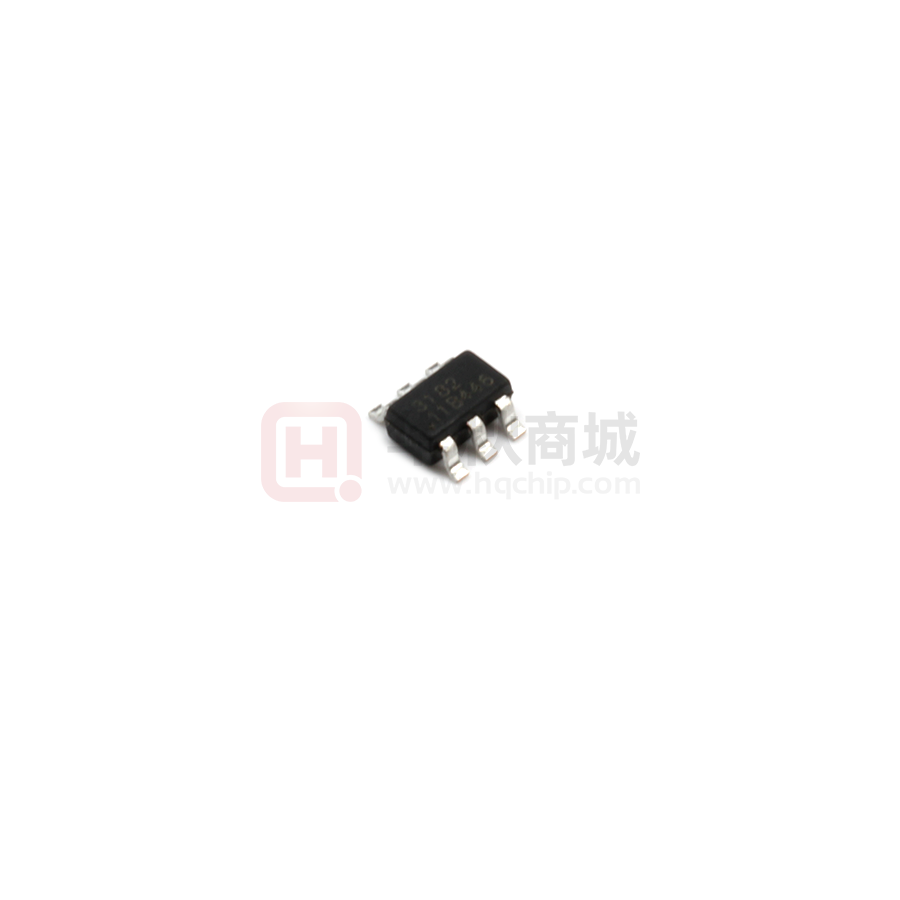
XP3182
FINE MADE MICROELECTRONICS GROUP
18V2A Synchronous Buck Converter
1 Features
2 Applications
Synchronous Buck Converter
- Internal Power MOSFET
- Wide 4.5V to 18V Input Voltage Range
- Output Current:2A
- 600KHZ frequency Operation
- 0.8V Reference
Distributed Power Systems
Digital Set Top Boxes
Flat Panel Television and Monitors
Notebook Computer
Wireless and DSL Modems
Efficiency @ Vout=5V
- Soft Start
100.00%
-Output Short With Hiccup Mode
90.00%
Multiple Protection
·
·
·
·
·
80.00%
- Input Over Voltage protection
VIN=12V
VIN=18V
70.00%
- Input Under Voltage protection
60.00%
- Output Over Voltage protection
50.00%
0
- Over Current protection With Hiccup
0.5
1
1.5
2
- Over Temperature Protection
3 Typical Application Circuit
4.5V~18V
C3 0.1uF
VIN
option
C1
BST
C2
4.7uF
SW
L1 4.7uH
R1
FB
VOUT
C3
22uF
R2
ON/
OFF
EN
GND
Note:The application scenario is that the DC power supply is directly plugged in, and it is
recommended to add electrolytic capacitance at the input.
1
www.superchip.cn No: S&CIC1928 Copyright © 2019, FINE MADE MICROELECTRONICSGROUP
�FINE MADE MICROELECTRONICS GROUP
XP3182
4 General Description
The XP3182B is a high frequency, synchronous buck converter with internal power
MOSFET. XP3182B supports wide input voltage range: 4.5V to 18V and provides 2.0A
continuous load current capability, and provide high efficiency without use of external
Schottky diode. Low output voltage ripple and small external inductor and capacitor size are
achieved with 600KHz switching frequency
XP3182B has a variety of protection functions:Input over voltage protection, Input
UVLO, Output over current protection, Output short protection and thermal shutdown.
The XP3182B is available in a 6-pin SOT23-6 package, which provides a compact
solution with minimal external components.
2
www.superchip.cn No: S&CIC1928 Copyright © 2019, FINE MADE MICROELECTRONICSGROUP
�XP3182
FINE MADE MICROELECTRONICS GROUP
5 Pin Description
BST
1
6
SW
GND
2
5
VIN
FB
3
4
EN
top view
Pin
Name
Function
Bootstrap. A capacitor connected between SW and BST pins is required
to form a floating supply across the high-side switch driver
Ground
1
BST
2
GND
3
FB
4
EN
5
VIN
Output Voltage feedback input
Drive this pin to a logic‐high to enable the IC. Drive to a logic‐low to
disable the IC and enter micro‐power shutdown mode
Power Supply Pin
6
SW
Switching Pin
6 Ordering Information
Part Number
Mark
Specification
Package
XP3182B
3182
XXXX
FB Reference : 0.8V
SOT23-6
Mark description:
First line:Device Code;
Second line, XXXX:Lot Number.
3
www.superchip.cn No: S&CIC1928 Copyright © 2019, FINE MADE MICROELECTRONICSGROUP
�XP3182
FINE MADE MICROELECTRONICS GROUP
7 Specification
7.1 Limit Operating Parameter (1)
Parameter
Min
Max
Unit
VIN
-0.3
20
V
VSW
-0.3
VIN
V
VBST
VSW-0.3
VSW+6
V
VFB
-0.3
6
V
VEN
-0.3
20
V
TJ
-40
150
℃
TSTG
-40
150
℃
(1) Permanent device damage may occur if Absolute Maximum Ratings are exceeded.
7.2 ESD Rating
Items
VESDHBM
Description
Human Body Model for all pin
Value
Unit
±2000
V
ESD test base on Human Body Model.
7.3 Recommended Operating Conditons
Parameter
Min
Typ
Max
Unit
VIN
4.5
12
18
V
L
4.7
µH
CIN
4.7
µF
COUT
22
µF
TA
-40
85
℃
Value
Unit
170
℃/W
7.4 Thermal Information
Parameter
RθJA
4
Description
Junction-to-ambient thermal resistance
www.superchip.cn No: S&CIC1928 Copyright © 2019, FINE MADE MICROELECTRONICSGROUP
�XP3182
FINE MADE MICROELECTRONICS GROUP
7.5 Electrical Characteristics
VIN=12V, VOUT=5V, L=4.7uH, Ta=25℃ , unless other notes
Parameters
Symbol
Condition
VIN Under Voltage
IUVLO
VIN=4V
Current
Quiescent Current
INOSW
VIN=12V
Supply Current in
ISD
VEN=0 or VEN=GND
Shutdown
FB Voltage Reference
VFB
XP3182B
Minimum Turn-on
VUVLO
Voltage
Maximum Turn-on
VINOVP
Voltage
High-Side Switch
RDSON_H
On-Resistance
Low-Side Switch
RDSON_L
On-Resistance
Frequency
FOSC
5
Min
Typ
Max
Unit
80
uA
500
uA
1
uA
0.8
V
4
V
18
V
100
mΩ
70
mΩ
600
kHz
Maximum Duty Cycle
DMAX
90
%
Minimum On Time
TON
100
ns
Minimum Off Time
TOFF
200
ns
Valley Current Limit
ICC
2.5
A
Soft Start Time
TSS
2
mS
Hiccup Time
THICCUP
120
mS
OTP
TSD
150
℃
www.superchip.cn No: S&CIC1928 Copyright © 2019, FINE MADE MICROELECTRONICSGROUP
�XP3182
FINE MADE MICROELECTRONICS GROUP
8 Detailed Description
8.1 Setting the output voltage
Vout
R1
FB
R2
Set the output voltage
The connection above shows the setting of the output voltage. The FB voltage of
XP3182B is 0.8V, The external resistor divider is used to set the output voltage.R1,R2 is
given by:
VOUT=0.8V*(R1+R2)/R2
Vout
5V
3.3V
1.8V
1.2V
6
R1(KΩ)
R2(KΩ)
100
100
100
100
19
32
80
200
www.superchip.cn No: S&CIC1928 Copyright © 2019, FINE MADE MICROELECTRONICSGROUP
�FINE MADE MICROELECTRONICS GROUP
XP3182
8.2 Selecting the inductor
For highest efficiency, the inductor DC resistance should be as low as possible. The
recommended inductor values are shown in the application diagram. It is important to
ensure that the inductor is not saturated in any situation.
L=VOUT*(VIN-VOUT)/(VIN*△IL *fOSC)
Where VIN is the input voltage, VOUT is the output voltage, fOSC is the switching
frequency, and △IL is the peak-to-peak inductor ripple current.
8.3 Layout Guide
1. Input capacitance and high frequency decoupling small capacitors should be as
close to the input pins as possible to improve filtering effect.
2. Inductor should be as close to the SW pin to reduce electromagnetic noise.
3. Output capacitance COUT should be as close to inductor.
4. Vout , SW away from sensitive analog areas such as FB.
7
www.superchip.cn No: S&CIC1928 Copyright © 2019, FINE MADE MICROELECTRONICSGROUP
�FINE MADE MICROELECTRONICS GROUP
XP3182
9 Package Information
8
www.superchip.cn No: S&CIC1928 Copyright © 2019, FINE MADE MICROELECTRONICSGROUP
�
很抱歉,暂时无法提供与“XP3182”相匹配的价格&库存,您可以联系我们找货
免费人工找货- 国内价格
- 5+0.56412
- 50+0.40167
- 600+0.32936
