RDA5820NS
SINGLE-CHIP BROADCAST FM TRANSCEIVER
1
Rev.1.1–Mar.2011
General Description
The RDA5820NS is the newest generation
single-chip broadcast FM receive/transmit tuner
with fully integrated synthesizer, IF selectivity and
MPX decoder. The chip uses the CMOS process,
support multi-interface and require the least
external component. The package size is 3X3mm
and is completely adjustment-free. All these make
it very suitable for portable devices.
The RDA5820NS has a powerful low-IF digital
audio processor, this make it have optimum sound
quality with varying reception conditions.
The RDA5820NS use RDA patented dual
synthesizers, all digital transmit structure, this
make it have perfectly transmition performance
and agility.
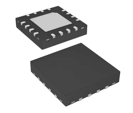
Figure 1-1. RDA5820NS Top View
The RDA5820NS support 50M~115M frequency band FM and RDS/RBDS receive and transmit, support
power supply range is 1.8-5.5V, all these make it can be used in simple wireless control appliance such
as mobile phone or toys.
The RDA5820NS package is pin-to-pin compatible with FM receive tuner RDA5802NS.
1.1
Features
CMOS single-chip fully-integrated FM transceiver
High performance A/D converter
Low power consumption
IF selectivity performed internally
Total current consumption is about 26 mA at
Fully integrated on-chip loop filter
3.0 V power supply (maximum power transmit
All digital transmitter
mode)
Autonomous search tuning
Support RDS/RBDS receive and transmit
Support SNR FM searching
Support 32.768KHz crystal oscillator
Digital auto gain control (AGC)
Digital adaptive noise cancellation
50 -115 MHz
100KHz, 200KHz, 50KHz and 25KHz
Digital low-IF tuner
Fully integrated digital frequency synthesizer
Fully integrated on-chip RF and IF VCO
Support flexible channel spacing mode
Support worldwide and campus frequency band
Total current consumption is about 22mA at
3.0 V power supply (receive mode)
Image-reject down-converter
Mono/stereo switch
Copyright © RDA Microelectronics Inc. 2006. All rights are reserved.
The information contained herein is the exclusive property of RDA and shall not be distributed, reproduced, or disclosed in whole or in
part without prior written permission of RDA.
�RDA Microelectronics, Inc.
Soft mute
High cut
Programmable de-emphasis (50/75 s)
Receive signal strength indicator (RSSI) and SNR
Bass boost
Volume control
Support I2S digital transmitter
Support audio power amplifier ( 32Ω resistance
loading)
I2S digital input / output interface
Line-level analog output voltage
32.768 KHz, 12M,24M,13M,26M,19.2M,38.4MHz
RDA5820NS FM Transceiver V1.1
1.8 to 5.5 V operation voltage
3X3mm 20 pin QFN package
Pin-to-pin compatible with RDA5802NS
1.2
Applications
Cellular handsets
MP3, MP4 players
Portable radios
PDAs, Notebook PCs
Wireless Toys
reference clock
Only support IIC serial control bus interface
Directly support 32Ω resistance loading
Integrated LDO regulator
The information contained herein is the exclusive property of RDA and shall not be distributed, reproduced, or disclosed in whole or in
part without prior written permission of RDA.
Page 2 of 28
�RDA Microelectronics, Inc.
RDA5820NS FM Transceiver V1.1
2
Table of Contents
1
General Description ....................................................................................................................................1
1.1
Features .........................................................................................................................................1
1.2
Applications ..................................................................................................................................2
Table of Contents.........................................................................................................................................2
Functional Description................................................................................................................................3
3.1
FM Transceiver Structure ..................................................................................................................3
3.2
FM Receive ...................................................................................................................................3
3.3
FM Transmit..................................................................................................................................4
3.4
Audio Amplify ..............................................................................................................................4
3.5
I2S Transmit ..................................................................................................................................4
3.6
PA..................................................................................................................................................4
3.7
Synthesizer1 ..................................................................................................................................4
3.8
Synthesizer2 ....................................................................................................................................4
3.9
Power Supply ................................................................................................................................4
3.10
RESET and Control Interface select .............................................................................................4
3.11
Control Interface ...........................................................................................................................4
3.12
I2S Audio Data Interface ...............................................................................................................5
3.13
GPIO Outputs................................................................................................................................5
Electrical Characteristics ...........................................................................................................................6
Receiver Characteristics .............................................................................................................................7
Transmitter Characteristics .......................................................................................................................9
6.1
I2C Interface Timing.................................................................................................................... 11
Register Definition ....................................................................................................................................12
Pins Description.........................................................................................................................................18
Application Diagram.................................................................................................................................21
9.1
RDA5820NS Common Application Diagram:............................................................................21
9.1.1
Bill of Materials: .........................................................................................................................21
Package Physical Dimension ....................................................................................................................22
PCB Land Pattern.....................................................................................................................................23
Change List................................................................................................................................................26
Notes: .......................................................................................................................................................26
Contact Information .................................................................................................................................27
2
3
4
5
6
7
8
9
10
11
12
13
14
The information contained herein is the exclusive property of RDA and shall not be distributed, reproduced, or disclosed in whole or in
part without prior written permission of RDA.
Page 2 of 28
�RDA Microelectronics, Inc.
RIN
Functional Description
LIN
3
RDA5820NS FM Transceiver V1.1
Figure 3-1. RDA5820NS FM Transceiver Block Diagram
3.1
FM Transceiver Structure
The RDA5820NS is a single-chip FM transceiver
(Rx/Tx).
Based
on
RDA
patented
dual
synthesizers RF structure, it has perfectly FM
receive and transmit performances, also least
external components.
Except FM receive and transmit, the RDA5820NS
also have RDS/RBDS, I2S input/output, audio
amplify functions. All these make it very suitable
for portable devices.
3.2
FM Receive
The receiver uses a digital low-IF architecture that
avoids the difficulties associated with direct
conversion while delivering lower solution cost
and reduces complexity, and integrates a low
noise amplifier (LNA) supporting the FM
broadcast band (50 to 115MHz), a quadrature
image-reject mixer, a programmable gain control
(PGA), a high resolution analog-to-digital
converters (ADCs), an audio DSP and a highfidelity digital-to-analog converters (DACs).
The LNA has differential input ports, which have
same characters and anyone of them can used as
FM signal input port. The two LNA ports can be
arbitrary selected by set according registers bits
(LNA_PORT_SEL[1:0]). It default input common
mode voltage is GND.
The quadrature mixer down converts the LNA
output differential RF signal to low-IF, it also has
image-reject function.
The PGA amplifies the mixer output IF signal and
then digitized with ADCs.
The DSP core finishes the channel selection, FM
demodulation, stereo MPX decoder and output
audio signal. The MPX decoder can autonomous
switch from stereo to mono to limit the output
noise.
The DACs convert digital audio signal to analog
and change the volume at same time. The DACs
has low-pass feature and -3dB frequency is about
30 KHz.
The PA (Power Amplifier) is power down. Its
output impedance is high resistance.
The information contained herein is the exclusive property of RDA and shall not be distributed, reproduced, or disclosed in whole or in
part without prior written permission of RDA.
Page 3 of 28
�RDA Microelectronics, Inc.
3.3
RDA5820NS FM Transceiver V1.1
FM Transmit
3.6
The transmit uses a digital modulate structure.
Audio signals (LIN and RIN) are amplified by
PGAs firstly, then converted to digital codes by
ADCs. The DSP core finishes audio coding and
FM modulate, pre-emphasis. The syntersizer2
transmits the digital FM data to VCO2. The PA
(Power Amplifier) amplify the FM signal.
The PGA gain and PA gain are adjustable by
set according registers bits (PGA_GAIN[2:0]
1
and PA_GAIN[5:0]2).
Table 3-1 PGA_GAIN and Input Signal Strength
PGA_GAIN[2:0]
V-LIN(VPP)
PGA_GAIN[2:0]
V-LIN(VPP)
000
1.20V
100
0.075V
001
0.60V
101
0.037V
010
0.30V
110
0.018V
011
0.15V
111
0.009V
PA
The PA (Power Amplifier) work frequency band is
50~115MHz, and output power is linearly
adjustable. The PA use linear structure for better
frequency distortion performance.
3.7
Synthesizer1
The
frequency
synthesizer
1
(including
synthesizer1 and VCO1 ) generates the local
oscillator signal which divide to quadrature, then
be used to downconvert the RF input to a
constant low intermediate frequency (IF). The
synthesizer reference clock is 32.768 KHz.
The synthesizer1 frequency is defined by bits
CHAN[9:0] with the range from 50MHz to
115MHz.
The synthesizer1 also generates reference to
synthesizer2 under FM TX (transmit) mode.
3.8
Synthesizer2
Table 3-2 PA_GAIN and Fm Transmit Power
PA_GAIN[5:0]
POUT
PA_GAIN[5:0]
POUT
111111
3dBm
011001
-3dBm
100111
0dBm
000000
-32dBm
3.4
Audio Amplify
Audio signals (LIN and RIN) can also directly
send to audio amplifier in DACs and driving the
headphone through LOUT and ROUT ports.
3.5
The frequency synthesizer 2 (including
synthesizer2 and VCO2 ) generates clock
signals for ADC under FM RX (receive) mode.
The frequency synthesizer2 is also the FM
transmit core. The digital signals (audio and
RDS/RBDS) are directly added on it.
3.9
Power Supply
The RDA5820NS integrated one LDO which
supplies power to the chip. The external supply
voltage range is 1.8-5.5 V.
I2S Transmit
3.10
The RDA5820NS supports directly digital FM
transmit. The digital signals can input through
chip’s ports GPIO1/2/3, then transmits directly
through synthersizer2 and PA, also transimts to
DAC and send out through LOUT and ROUT
ports. I2S mode support slave mode.
RESET and Control Interface select
The RDA5820NS is RESET itself When VIO is
Power up. And also support soft reset by trigger
02H BIT1 from 0 to 1.
3.11
Control Interface
The RDA5820NS only supports I2C control
interface.
1
2
Register 0x68H_BIT[12:10]
Register 0x41H_BIT[5:0]
PGA_GAIN_BIT[2:0]
PA_GAIN_BIT[2:0]
The I2C
interface is compliant to I2C Bus
Specification 2.1. It includes two pins: SCLK and
The information contained herein is the exclusive property of RDA and shall not be distributed, reproduced, or disclosed in whole or in
part without prior written permission of RDA.
Page 4 of 28
�RDA Microelectronics, Inc.
RDA5820NS FM Transceiver V1.1
SDIO. A I2C interface transfer begins with START
42Kbps.
condition, a command byte and data bytes, each
byte has a followed ACK (or NACK) bit, and ends
with STOP condition. The command byte includes
a 7-bit chip address (0010001b) and a R/W bit.
The ACK (or NACK) is always sent out by receiver.
When in write transfer, data bytes is written out
from MCU, and when in read transfer, data bytes
is read out from RDA5820NS.
3.12
I2S Audio Data Interface
The RDA5820NS supports I2S (Inter_IC Sound
Bus) audio interface. The interface is fully
compliant with I2S bus specification. When setting
I2SEN bit high, RDA5820NS will output SCK, WS,
SD signals from GPIO3, GPIO1, GPIO2 as I2S
master and transmitter, the sample rate is
3.13
GPIO Outputs
The RDA5820NS has three GPIOs. The function
of GPIOs could programmed with bits GPIO1[1:0],
GPIO2[1:0], GPIO3[1:0] and I2SEN.
If I2SEN is set to low, GPIO pins could be
programmed to output low or high or high-Z, or be
programmed to output interrupt and stereo
indicator with bits GPIO1[1:0], GPIO2[1:0],
GPIO3[1:0]. GPIO2 could be programmed to
output a low interrupt (interrupt will be generated
only with interrupt enable bit STCIEN is set to high)
when seek/tune process completes. GPIO3 could
be programmed to output stereo indicator bit ST.
Constant low, high or high-Z functionality is
available regardless of the state of VDD supplies
or the ENABLE bit.
SCK
WS
LEFT CHANNEL
RIGHT CHANNEL
1 SCK
SD
1 SCK
MSB
LSB
MSB
LSB
Figure 3-2. I2S Digital Audio Format
The information contained herein is the exclusive property of RDA and shall not be distributed, reproduced, or disclosed in whole or in
part without prior written permission of RDA.
Page 5 of 28
�RDA Microelectronics, Inc.
4
RDA5820NS FM Transceiver V1.1
Electrical Characteristics
Table 4-1
DC Electrical Specification (Recommended Operation Conditions):
SYMBOL
DESCRIPTION
MIN
TYP
MAX
UNIT
VDD
Supply Voltage
1.8
3.3
5.5
V
VIO
Interface Supply Voltage
1.5
-
3.6
V
Tamb
Ambient Temperature
-20
27
+70
℃
VIL
CMOS Low Level Input Voltage
0
0.3*VIO
V
VIH
CMOS High Level Input Voltage
0.7*VIO
VIO
V
VTH
CMOS Threshold Voltage
Table 4-2
0.5*VIO
V
DC Electrical Specification (Absolute Maximum Ratings):
SYMBOL
DESCRIPTION
MIN
TYP
MAX
UNIT
VIO
Interface Supply Voltage
-0.5
+4
V
Tamb
Ambient Temperature
IIN
-40
+90
°C
(1)
-10
+10
mA
(1)
-0.3
VIO+0.3
V
0
dBm
Input Current
VIN
Input Voltage
Vlna
LNA FM Input Level
Notes:
1. For Pin: SCLK, SDIO
Table 4-3
Power Consumption Specification
(VDD = 3 V, VIO=3 V, TA =25℃, unless otherwise specified)
SYMBOL
DESCRIPTION
CONDITION
TYP
UNIT
FM Receive
IVDD
Supply Power Current
ENABLE=1
22
mA
IVIO
Interface Supply Current
SCLK and RCLK inactive
200
A
IAPD
Analog Powerdown Current
ENABLE=0
5
A
IDPD
Digital Powerdown Current
ENABLE=0
10
A
IVDD
Supply Power Current
PA_GAIN[5:0]=[111111];VRF=3dBm
26
mA
IVDD
Supply Power Current
PA_GAIN[5:0]=[100111];VRF=0dBm
25
mA
IVDD
Supply Power Current
PA_GAIN[5:0]=[011001];VRF=3dBm
24.5
mA
IVDD
Supply Power Current
PA_GAIN[5:0]=[000000];VRF=-32dBm
23
mA
FM Transmit
The information contained herein is the exclusive property of RDA and shall not be distributed, reproduced, or disclosed in whole or in
part without prior written permission of RDA.
Page 6 of 28
�RDA Microelectronics, Inc.
5
RDA5820NS FM Transceiver V1.1
Receiver Characteristics
Table 5-1
Receiver Characteristics
(VDD = 3 V, VIO=3 V, TA = 25 °C, unless otherwise specified)
SYMBOL
PARAMETER
CONDITIONS
MIN
Adjust BAND Register
50
TYP
MAX
UNIT
115
MHz
General Specifications
Fin
FM Input Frequency Range
1,2,3
Vrf
S/N=26dB
Sensitivity
IFrej
Iimage_rej
Input IP3
-
1.2
98MHz
-
1.2
108MHz
-
1.3
AGCD=1
80
m=0.3
60
±200KHz
±400KHz
1,2
AM Suppression
Adjacent Channel
Selectivity
VAFR
(Pins LOUT and ROUT)
EMF
6
Ratio
Stereo
Stereo Channel Separation
Audio Output Loading
Single-ended
Resistance
Audio Total Harmonic
1,3,6
Distortion
Volume[3:0]=1111
-
Db
50
70
-
Db
60
85
mV
55
57
-
53
55
35
-
-
dB
32
-
-
Ω
0.03
0.05
-
-
0.05
dB
60
-
-
dB
Rload=32Ω
Imbalance1,6
Audio Response1
-
Rload=1KΩ
Audio Output L/R
Mute Attenuation Ratio1
dBV
420
Mono2
1,2,3,5
BWaudio
V
-
Volume [3 :0] =1111
Maximum Signal to Noise
αAOI
Rmute
88MHz
dB
Audio L/R Output Voltage
THD
1.2
40
VAFL;
RL
-
Image Rejection
400KHz Selectivity
αSCS
65MHz
dB
S400
S/N
1.5
40
IP3in
S200
-
IF Rejection
4
αam
50MHz
Volume[3:0]=0000
9
1KHz=0dB ± 3dB
Low Freq
100
point
High Freq
14
dB
%
Hz
Pins FMIN,FMOUT, LOUT, ROUT,LIN,RIN
Vcom_fmin
Vcom_fmout
Vcom_in
Vcom
Pins
FMIN
Input
Common
Mode
V
0
Voltage
Pin FMOUT Common Mode Voltage
V
0
Pins LIN/RIN Input Common Mode
Audio Output Common Mode Voltage8
V
1.1
Voltage
0.95
1.
1.05
V
The information contained herein is the exclusive property of RDA and shall not be distributed, reproduced, or disclosed in whole or in
part without prior written permission of RDA.
Page 7 of 28
�RDA Microelectronics, Inc.
RDA5820NS FM Transceiver V1.1
Notes:
1. Fin=65 to 115MHz; Fmod=1KHz; de-emphasis=75s; MONO=1; L=R unless noted otherwise;
2. f=22.5KHz;
3. BAF = 300Hz to 15KHz, RBW 1MHz, f0=2xf1-f2, AGC disable, Fin=76 to 108MHz;
5. PRF=60dBUV;
6. f=75KHz.
7. Measured at VEMF = 1 m V, f RF = 76 to 108MHz
8. At LOUT and ROUT pins
9.Adjustable
The information contained herein is the exclusive property of RDA and shall not be distributed, reproduced, or disclosed in whole or in
part without prior written permission of RDA.
Page 8 of 28
�RDA Microelectronics, Inc.
6
RDA5820NS FM Transceiver V1.1
Transmitter Characteristics
Table 6-1
Transmitter Characteristics
(VDD = 3 V, VIO=3 V, TA = 25 °C, unless otherwise specified)
SYMBOL
PARAMETER
CONDITIONS
MIN
TYP
MAX
UNIT
115
MHz
General specifications
Frf
△
F
Transmit Frequency
50
2,3
Transmit Frequency Accuracy and Stability
2.6
KHz
VRF
Maximum Transmit Voltage
PA_GAIN=[111111]
3
dBm
VRF
Minimum Transmit Voltage
PA_GAIN=[000000]
-32
dBm
Transmit Voltage Step
3
dBm
Transmit Voltage Stability
1
dB
Transmit Channel
>±100KHz
Edge Power
Pre-emphasis off
Transmit Adjacent
>±200KHz
Channel Power
Pre-emphasis off
Transmit Alternate
>±400KHz
Channel Power
Transmit Emissions
Pre-emphasis off
In band(76 to 108MHz)
-85
dBc
-85
dBc
-85
dBc
-50
dBc
Pre-emphasis
TX_PREMPHASIS=75 us
70
75
80
us
Time Constant
TX_PREMPHASIS=50 us
45
50
55
us
50
55
dB
51
55
dB
f=22.5KHz,Mono
△
Audio SNR Mono
Limiter off
f=22.5KHz,
△
fpolit=6.75KHz,
△
Audio SNR Stereo
Stereo
Limiter off
f=75KHz,Mono
△
Audio THD Mono
Limiter off
0.08
0.6
%
0.08
0.6
%
f=68.25KHz,
△
fpolit=6.75KHz,
△
Audio THD Stereo
Stereo
Limiter off
SCR
Audio Stereo Separation
40
dB
Sub Carrier Rejection Ratio
27
dB
Power up Setting Time
30
ms
Input Signal Level
1
VPK
15K
Hz
Mono,±1.5dB,
Frequency Flatness
f=75KHz,
△
0,50,75us pre-emphasis,
30
limiter off
The information contained herein is the exclusive property of RDA and shall not be distributed, reproduced, or disclosed in whole or in
part without prior written permission of RDA.
Page 9 of 28
�RDA Microelectronics, Inc.
RDA5820NS FM Transceiver V1.1
Mono,-3dB,
High-Pass
△
Frequency Response
0,50,75us pre-emphasis,
f=75KHz,
5
30
Hz
15k
16k
Hz
-1
1
dB
-10
10
%
-10
10
%
limiter off
Mono,-3dB,
Low-Pass
△
Frequency Response
0,50,75us pre-emphasis,
f=75KHz,
limiter off
Audio Imbalance
Mono
Pilot Modulation
△
Rate Accuracy
△
Audio Modulation
△
Rate Accuracy
△
f=68.25KHz,
fpilot=6.75KHz,Stereo
f=68.25KHz,
fpilot=6.75KHz,Stereo
Input Resistance
10
15
20
K
Input Capacitance
0.5
0.7
1
pF
Notes:
1. Fin=65 to 115MHz; Fmod=1KHz; de-emphasis=75s; MONO=1; L=R unless noted otherwise;
2.Guaranteed by Characterization only ;
3.No measurable △fRF/△VDD at
VDD of 500mV pk-pk at 100HZ to 10KHz;
△
The information contained herein is the exclusive property of RDA and shall not be distributed, reproduced, or disclosed in whole or in
part without prior written permission of RDA.
Page 10 of 28
�RDA Microelectronics, Inc.
RDA5820NS FM Transceiver V1.1
Serial Interface
6.1
I2C Interface Timing
Table 6-1
I2C Interface Timing Characteristics
(VDD = 3 V, VIO=3 V, TA = 25°C, unless otherwise specified)
PARAMETER
SYMBOL
TEST CONDITION
MIN
TYP
MAX
UNIT
SCLK Frequency
fscl
0
-
400
KHz
SCLK High Time
thigh
0.6
-
-
s
SCLK Low Time
tlow
1.3
-
-
s
Setup Time for START Condition
tsu:sta
0.6
-
-
s
Hold Time for START Condition
thd:sta
0.6
-
-
s
Setup Time for STOP Condition
tsu:sto
0.6
-
-
s
SDIO Input to SCLK↑ Setup
tsu:dat
100
-
-
ns
SDIO Input to SCLK↓ Hold
thd:dat
0
-
900
ns
STOP to START Time
tbuf
1.3
-
-
s
SDIO Output Fall Time
tf:out
20+0.1Cb
-
250
ns
tr:in / tf:in
20+0.1Cb
-
300
ns
Input Spike Suppression
tsp
-
-
50
ns
SCLK, SDIO Capacitive Loading
Cb
-
-
50
pF
5
pF
SDIO Input, SCLK Rise/Fall Time
Digital Input Pin Capacitance
Figure 6-1. I2C Interface Write Timing Diagram
Figure 6-2. I2C Interface Read Timing Diagram
The information contained herein is the exclusive property of RDA and shall not be distributed, reproduced, or disclosed in whole or in
part without prior written permission of RDA.
Page 11 of 28
�RDA Microelectronics, Inc.
7
Register Definition
REG
00H
02H
RDA5820NS FM Transceiver V1.1
BITS
15:0
15
NAME
FUNCTION
DEFAULT
CHIPID[15:0]
Chip ID.
0x5820
DHIZ
Audio Output High-Z Disable.
0
0 = High impedance; 1 = Normal operation
14
Mute Disable.
DMUTE
0
0 = Mute; 1 = Normal operation
13
Mono Select.
MONO
0
0 = Stereo; 1 = Force mono
12
BASS
11
RCLK
Bass Boost.
0
0 = Disabled; 1 = Bass boost enabled
NON-CALIBRATE
0=RCLK clock is always supply
0
1=RCLK clock is not always supply when FM work ( when
MODE
1,
RDA5820NS
can’t
directly
support
-20℃~70℃
temperature. Only suppory ±20℃ temperature swing from
tune point)
10
RCLK
DIRECT
INPUT
1=RCLK clock use the directly input mode
0
0
MODE
9
SEEKUP
Seek Up.
8
SEEK
Seek.
0 = Seek down; 1 = Seek up
0
0 = Disable stop seek; 1 = Enable
Seek begins in the direction specified by SEEKUP and
ends when a channel is found, or the entire band has been
searched.
The SEEK bit is set low and the STC bit is set high when
the seek operation completes.
7
SKMODE
Seek Mode
0
0 = wrap at the upper or lower band limit and continue
seeking
1 = stop seeking at the upper or lower band limit
6:4
CLK_MODE[2:0]
000=32.768kHz
000
001=12Mhz
101=24Mhz
010=13Mhz
110=26Mhz
011=19.2Mhz
111=38.4Mhz
3
RDS_EN
RDS/RBDS enable
0
If 1, RDS/RBDS enable
2
RSVD
Reserved
0
1
SOFT_RESET
Soft reset.
0
If 0, not reset;
If 1, reset.
The information contained herein is the exclusive property of RDA and shall not be distributed, reproduced, or disclosed in whole or in
part without prior written permission of RDA.
Page 12 of 28
�RDA Microelectronics, Inc.
REG
BITS
0
RDA5820NS FM Transceiver V1.1
NAME
ENABLE
FUNCTION
Power Up Enable.
DEFAULT
0
0 = Disabled; 1 = Enabled
03H
15:6
CHAN[9:0]
Channel Select.
0x00
BAND = 0
Frequency =
Channel Spacing (kHz) x CHAN+ 87.0 MHz
BAND = 1or 2
Frequency =
Channel Spacing (kHz) x CHAN + 76.0 MHz
BAND = 3
Frequency =
Channel Spacing (kHz) x CHAN + 65.0 MHz
CHAN is updated after a seek operation.
5
DIRECT MODE
Directly Control Mode, Only used when test.
0
4
TUNE
Tune
0
0 = Disable
1 = Enable
The tune operation begins when the TUNE bit is set high.
The STC bit is set high when the tune operation completes.
The tune bit is reset to low automatically when the tune
operation completes..
3:2
BAND[1:0]
Band Select.
00
00 = 87–108 MHz (US/Europe)
01 = 76–91 MHz (Japan)
10 = 76–108 MHz (world wide)
3
11 = 65 –76 MHz (East Europe) or 50-65MHz
1:0
SPACE[1:0]
Channel Spacing.
00
00 = 100 kHz
01 = 200 kHz
10 = 50kHz
11 = 25KHz
04H
15
RDSIEN
RDS ready Interrupt Enable.
0
0 = Disable Interrupt
1 = Enable Interrupt
Setting STCIEN = 1 will generate a low pulse on GPIO2
when the interrupt occurs.
14
STCIEN
Seek/Tune Complete Interrupt Enable.
0
0 = Disable Interrupt
1 = Enable Interrupt
Setting STCIEN = 1 will generate a low pulse on GPIO2
when the interrupt occurs.
13
RBDS
1 = RBDS mode enable
0
0 = RDS mode only
12
3
RDS_FIFO_EN
1 = RDS fifo mode enable.
0
If 0x07h_bit[9] ( band )=1, 65-76MHz; =0, 50-76MHz
The information contained herein is the exclusive property of RDA and shall not be distributed, reproduced, or disclosed in whole or in
part without prior written permission of RDA.
Page 13 of 28
�RDA Microelectronics, Inc.
REG
BITS
11
RDA5820NS FM Transceiver V1.1
NAME
FUNCTION
De-emphasis.
DE
DEFAULT
0
0 = 75 µs; 1 = 50 µs
10
RDS_FIFO_CLR
1 = clear RDS fifo
1
9
SOFTMUTE_EN
If 1, softmute enable
1
8
AFCD
AFC disable.
0
If 0, afc work;
If 1, afc disabled.
7
RSVD
Reserved
0
6
I2S_ENABLED
I2S bus enable
0
If 0, disabled;
If 1, enabled.
5:4
General Purpose I/O 3.
GPIO3[1:0]
00
00 = High impedance
01 = Mono/Stereo indicator (ST)
10 = Low
11 = High
3:2
General Purpose I/O 2.
GPIO2[1:0]
00
00 = High impedance
01 = Interrupt (INT)
10 = Low
11 = High
1:0
General Purpose I/O 1.
GPIO1[1:0]
00
00 = High impedance
01 = Reserved
10 = Low
11 = High
05H
15
INT _MODE
If 0, generate 5ms interrupt;
1
If 1, interrupt last until read reg0CH action occurs.
14:13
SEEK_MODE[1:0]
01= adjacent seek process && noise condition
00
10= adjacent seek process || noise condition
12
11:8
RSVD
SEEKTH[3:0]
4
(inverse
of
Reserved
0
Seek SNR threshold value:
1000
Noise_th(dB) = 79 – seek_th
noise_h_th)
7:6
LNA_PORT_SEL[1:0]
LNA input port selection bit:
10
00: no input
01: LNAN
10: LNAP
11: dual port input
5:4
RSVD
Reserved
00
3:0
VOLUME[3:0]
DAC Gain Control Bits (Volume).
1111
0000=min; 1111=max
Volume scale is logarithmic
When 0000, output mute and output impedance is very
large
4
The default noise threshold is 71dB.
The information contained herein is the exclusive property of RDA and shall not be distributed, reproduced, or disclosed in whole or in
part without prior written permission of RDA.
Page 14 of 28
�RDA Microelectronics, Inc.
REG
06H
BITS
15:13
12
RDA5820NS FM Transceiver V1.1
NAME
FUNCTION
RSVD
I2S_MODE
5
DEFAULT
reserved
000
If 0, master mode;
0
If 1, slave mode.
11
3
SW_LR
Ws relation to l/r channel.
10
If 0, ws=0 ->r, ws=1 ->l;
If 1, ws=0 ->l, ws=1 ->r.
10
SCLK_I_EDGE
3
When I2S enable
0
If 0, use normal sclk internally;
If 1, inverte sclk internally.
9
DATA_SIGNED
3
If 0, I2S output unsigned 16-bit audio data.
0
If 1, I2S output signed 16-bit audio data.
8
WS_I_EDGE
3
If 0, use normal ws internally;
0
If 1, inverte ws internally.
7:4
3
I2S_SW_CNT[4:0]
( Only valid in master
mode )
3
2
1
07H
SW_O_EDGE
3
SCLK_O_EDGE
L_DELY
3
4'b1000: WS_STEP_48;
4'b0111: WS_STEP=44.1kbps;
4'b0110: WS_STEP=32kbps;
4'b0101: WS_STEP=24kbps;
4'b0100: WS_STEP=22.05kbps;
4'b0011: WS_STEP=16kbps;
4'b0010: WS_STEP=12kbps;
4'b0001: WS_STEP=11.025kbps;
4'b0000: WS_STEP=8kbps;
0000
If 1, invert ws output when as master.
0
If 1, invert sclk output when as master.
0
3
If 1, L channel data delay 1T.
0
3
If 1, R channel data delay 1T.
0
0
R_DELY
15
RSVD
Must be 0
0
14:10
TH_SOFRBLEND[5:0]
Softblend threshold setting for noise.
10011
If (127-noise_db2)>4*th, turn soft blend off.
9
65M_50M MODE
Valid when band[1:0] = 2’b11 (0x03H_bit)
1
1 = 65~76 MHz;
0 = 50~76 MHz.
8
7:2
RSVD
SEEK_TH_OLD
Reserved
6
Seek
threshold
0
for
old
seek
mode,
Valid
when
000000
Seek_Mode=01
1
SOFTBLEND_EN
If 1, Softblend enable
1
0
FREQ_MODE
If 1, then freq setting changed.
0
Freq = 76000(or 87000) kHz + freq_direct (08H) kHz.
0AH
15
RDSR
RDS ready
0
0 = No RDS/RBDS group ready(default)
1 = New RDS/RBDS group ready
14
STC
Seek/Tune Complete.
0
0 = Not complete
1 = Complete
3 This function is open when I2S_Enabled=1.
6
0x05H_bit[14:13], SEEK_MODE register. Default value is 00; When = 01, will add the 5802E seek mode.
The information contained herein is the exclusive property of RDA and shall not be distributed, reproduced, or disclosed in whole or in
part without prior written permission of RDA.
Page 15 of 28
�RDA Microelectronics, Inc.
REG
BITS
RDA5820NS FM Transceiver V1.1
NAME
FUNCTION
DEFAULT
The seek/tune complete flag is set when the seek or tune
operation completes.
13
SF
0
Seek Fail.
0 = Seek successful; 1 = Seek failure
The seek fail flag is set when the seek operation fails to
find
a
channel
with
an
RSSI
level
greater
than
SEEKTH[5:0].
12
RDSS
RDS Synchronization
0
0 = RDS decoder not synchronized(default)
1 = RDS decoder synchronized
Available only in RDS Verbose mode
11
BLK_E
When RDS enable:
0
1 = Block E has been found
0 = no Block E has been found
10
ST
1
Stereo Indicator.
0 = Mono; 1 = Stereo
Stereo indication is available on GPIO3 by setting
GPIO3[1:0] =01.
9:0
READCHAN[9:0]
Read Channel.
8’h00
BAND = 0
Frequency = Channel Spacing (kHz) x READCHAN[9:0]+
87.0 MHz
BAND = 1 or 2
Frequency = Channel Spacing (kHz) x READCHAN[9:0]+
76.0 MHz
BAND = 3
Frequency = Channel Spacing (kHz) x READCHAN[9:0]+
65.0 MHz
READCHAN[9:0] is updated after a tune or seek operation.
0BH
15:9
RSSI[6:0]
RSSI.
0
000000 = min
111111 = max
RSSI scale is logarithmic.
8
FM TRUE
1 = the current channel is a station
0
0 = the current channel is not a station
7
FM_READY
1=ready
0
0=not ready
6:5
RSVD
Reserved
00
4
ABCD_E
1= the block id of register 0cH,0dH,0eH,0fH is E
0
0= the block id of register 0cH, 0dH, 0eH,0fH is A, B, C, D
3:2
BLERA[1:0]
Block Errors Level of RDS_DATA_0,
and is always read as
00
Errors Level of RDS BLOCK A (in RDS mode) or BLOCK E
(in RBDS mode when ABCD_E flag is 1)
00= 0 errors requiring correction
01= 1~2 errors requiring correction
10= 3~5 errors requiring correction
11= 6+ errors or error in checkword, correction not
The information contained herein is the exclusive property of RDA and shall not be distributed, reproduced, or disclosed in whole or in
part without prior written permission of RDA.
Page 16 of 28
�RDA Microelectronics, Inc.
REG
BITS
RDA5820NS FM Transceiver V1.1
NAME
FUNCTION
DEFAULT
possible.
Available only in RDS Verbose mode
1:0
BLERB[1:0]
Block Errors Level of RDS_DATA_1, and is always read as
00
Errors Level of RDS BLOCK B (in RDS mode ) or E (in
RBDS mode when ABCD_E flag is 1).
00= 0 errors requiring correction
01= 1~2 errors requiring correction
10= 3~5 errors requiring correction
11= 6+ errors or error in checkword, correction not
possible.
Available only in RDS Verbose mode
0CH
15:0
RDSA[15:0]
BLOCK A ( in RDS mode) or BLOCK E (in RBDS mode when
16’h5820
ABCD_E flag is 1)
0DH
15:0
RDSB[15:0]
BLOCK B ( in RDS mode) or BLOCK E (in RBDS mode when
16’h5820
ABCD_E flag is 1)
0EH
15:0
RDSC[15:0]
BLOCK C ( in RDS mode) or BLOCK E (in RBDS mode when
16’h5805
ABCD_E flag is 1)
0FH
15:0
RDSD[15:0]
BLOCK D ( in RDS mode) or BLOCK E (in RBDS mode when
16’h5805
ABCD_E flag is 1)
40H
15:4
RSVD
3:0
WORK
MODE
Reserved
16’h000
0000 = FM Receive
0000
0001 = FM Transmit
1000 = Audio Amplify
1100 = Codec
1110 = ADC
41H
67H
68H
15:12
RSVD
Reserved
0000
11:9
TXPA_VCOM[2:0]
TXPA Common Voltage
000
8:6
TXPA_IBIT[2:0]
TXPA Bias Current
111
5:0
TXPA_GAIN[5:0]
TXPA Gain Bit
000000
15:8
FMTX_PILOT_DEV[7:0]
FM Transmit Pilot Tone Modulate Parameter
16’h0E
7:0
FMTX_RDS_ DEV[7:0]
FM Transmit RDS Signal Modulate Parameter
16’h10
RSVD
Reserved
00
FMTX_PGA_GAIN
FM Transmit PGA Gain Bit
001
FMTX_ADC_GAIN
FM Transmit ADC Gain Bit
000
FMTX_AUDIO_DEV
FM Transmit Audio Signal Modulate Parameter
16’hF0
The information contained herein is the exclusive property of RDA and shall not be distributed, reproduced, or disclosed in whole or in
part without prior written permission of RDA.
Page 17 of 28
�RDA Microelectronics, Inc.
GPIO2
VDD
RIN
RCLK
GPIO1
LIN
SDIO
VIO
GND
Pins Description
SCLK
8
RDA5820NS FM Transceiver V1.1
Figure 8-1. RDA5820NS Top View
Table 8-1
RDA5820NS Pins Description
SYMBOL
PIN
DESCRIPTION
GND
2,4,5,11,14,20,21
FMIN
3
FM LNAP input port.
FMOUT
1
.FM output port and LNAN input port
SCLK
SDIO
RCLK
VIO
VDD
ROUT,LOUT
RIN,LIN
GPIO1/2/3
6
7
8
9
10
12,13
18,19
17,16,15
Ground. Connect to ground plane on PCB
Clock input for serial control bus
Data input/output for serial control bus
32.768KHz crystal oscillator and reference clock input
Power supply for I/O
Power supply for analog and digital section
Right/Left audio output port
Right/Left audio input port
General purpose input/output
The information contained herein is the exclusive property of RDA and shall not be distributed, reproduced, or disclosed in whole or in
part without prior written permission of RDA.
Page 18 of 28
�RDA Microelectronics, Inc.
Table 8-2
Internal Pin Configuration
SYMBOL
FMIN
PIN
DESCRIPTION
4
17/18
Rload
RIN/LIN
RDA5820NS FM Transceiver V1.1
FMs
FMOUT
1
FMOUT
MN1
35pF
Sout
RCLK
8
The information contained herein is the exclusive property of RDA and shall not be distributed, reproduced, or disclosed in whole or in
part without prior written permission of RDA.
Page 19 of 28
�RDA Microelectronics, Inc.
SCLK/SDIO
RDA5820NS FM Transceiver V1.1
9/10
in
GPIO1/GPIO2/GPIO3
17/16/15
GPIO1\2\3
Out
The information contained herein is the exclusive property of RDA and shall not be distributed, reproduced, or disclosed in whole or in
part without prior written permission of RDA.
Page 20 of 28
�RDA Microelectronics, Inc.
9
RDA5820NS FM Transceiver V1.1
Application Diagram
9.1
RDA5820NS Common Application Diagram:
F1 1.5K@100MHz C4 125uF
J1 F2
Notes:
1. J1: Common 32Ω Resistance
1.5K@100MHz C5 125uF
FM_LIN
C7
Headphone;
2. U1: RDA5820NS Chip;
FM_RIN
C8
GPIO1
GPIO2
3.VDD: Power Supply (1.8~5.5V);
4: C7/C8: Audio Input Couple
Capacitance;
C1 1nF
1
5. FM Choke (L3 and C3) for Audio
GPIO3
Common;
6.C1: Fm Antenna Couple Capacitor
7. Place C6 Close to VDD pin.
8.Ferrite F1/F2 should close to J1.
11
SCLK
SDIO
RCLK
VIO
C6
24nF
V1
Figure 9-1. RDA5820NS FM Transceiver Application Diagram (TCXO Application)
9.1.1
Bill of Materials:
COMPONENT
U1
VALUE
RDA5820NS
J1
DESCRIPTION
Broadcast FM Transceiver
SUPPLIER
RDA
Common 32Ω Resistance Headphone
F1/F2
1.5K@100MHz
FM Band Ferrite
Murata
C1
1nF
FM Antenna Couple Capacitor
Murata
C7/C8
0.22uF
Audio Couple Capacitors
Murata
L3/C3
100nH/24pF
LC Chock for LNA Input
Murata
C4,C5
125µF
Audio AC Couple Capacitors
Murata
C6
24nF
Power Supply Bypass Capacitor
Murata
The information contained herein is the exclusive property of RDA and shall not be distributed, reproduced, or disclosed in whole or in
part without prior written permission of RDA.
Page 21 of 28
�RDA Microelectronics, Inc.
RDA5820NS FM Transceiver V1.1
10 Package Physical Dimension
Figure 10-1 illustrates the package details for the RDA5820NS. The package is lead-free and
RoHS-compliant.
Figure 10-2. 20-Pin 3x3 Quad Flat No-Lead (QFN)
The information contained herein is the exclusive property of RDA and shall not be distributed, reproduced, or disclosed in whole or in
part without prior written permission of RDA.
Page 22 of 28
�RDA Microelectronics, Inc.
RDA5820NS FM Transceiver V1.1
11 PCB Land Pattern
Figure 18.Classification Reflow Profile
Profile Feature
Sn-Pb Eutectic Assembly
Pb-Free Assembly
Average Ramp-Up Rate
3 oC/second max.
3 oC/second max.
-Temperature Min (Tsmin)
100 oC
150 oC
-Temperature Max (Tsmax)
100 oC
200 oC
-Time (tsmin to tsmax)
60-120 seconds
60-180 seconds
-Temperature (TL)
183 oC
217oC
-Time (tL)
60-150seconds
60-150 seconds
Peak /Classification
Temperature(Tp)
See Table-II
See Table-III
Time within 5 oC of actual
Peak Temperature (tp)
10-30 seconds
20-40 seconds
Ramp-Down Rate
6 oC/second max.
6 oC/seconds max.
Time 25 oC to Peak
Temperature
6 minutes max.
8 minutes max.
(TSmax to Tp)
Preheat
Time maintained above:
Table-I Classification Reflow Profiles
The information contained herein is the exclusive property of RDA and shall not be distributed, reproduced, or disclosed in whole or in
part without prior written permission of RDA.
Page 23 of 28
�RDA Microelectronics, Inc.
RDA5820NS FM Transceiver V1.1
Volume mm3
Volume mm3