0
登录后你可以
  • 下载海量资料
  • 学习在线课程
  • 观看技术视频
  • 写文章/发帖/加入社区
会员中心
创作中心
发布
  • 发文章

  • 发资料

  • 发帖

  • 提问

  • 发视频

创作活动
SY7088DGC

SY7088DGC

  • 厂商:

    SILERGY(矽力杰)

  • 封装:

    DFN8_2X3MM_EP

  • 描述:

    2.3V最小输入和5.5V最大输出3A峰值电流同步升压,输出断开

  • 详情介绍
  • 数据手册
  • 价格&库存
SY7088DGC 数据手册
昱灿电子 www.szyucan.com  Application Note: SY7088 2.3V Minimum Input and 5.5V Maximum Output 3A Peak Current Synchronous Boost with Output Disconnect Preliminary Specification General Description Features SY7088 is a high efficiency synchronous boost regulator that converts up to 5.5V output voltage. It adopts NMOS for the main switch and PMOS for the synchronous switch. It can disconnect the output from input during the shutdown mode. Ordering Information SY7088 □(□□ □□)□ □□ □ Tempera ture Code Packa ge Code Optiona l Spec Code Ordering Number SY7088DGC Package type DFN2x3-8 • • • • • • • • 2.3-5.0V input voltage range Adjustable output voltage from 2.5V to 5.5V Pseudo-constant frequency: 1MHz 3A peak current limit Input under voltage lockout Load disconnect during shutdown Output over voltage protection Low RDS(ON) (main switch/synchronous switch) at 5.0V output: 70/100mohm • Compact package: DFN2x3-8 Applications Note ---- • All Single Cell Li or Dual Cell Battery Operated Products as MP-3 Player, PDAs, and Other Portable Equipment. Typical Applications Figure 1. Schematic Diagram AN_SY7088 Rev. 0.1A Figure 2. Efficiency Figure 1 昱灿电子 www.szyucan.com  SY7088 Pinout (top view) (DFN2x3-8) Top mark: VTxyz (Device code: VT, x=year code, y=week code, z= lot number code) Name LX EN SGND DFN2x3-8 1, 2 3 4 FB 5 IN 6 OUT PGND 7, 8 9 Description Inductor node. Connect an inductor between IN pin and LX pin. Enable pin. Internal integrated with 1Mohm pull down resistor. Signal ground pin. Feedback pin. Connect a resistor RH between OUT and FB, and a resistor RL between FB and GND to program the output voltage. VOUT=1.2V*(RH/RL+1). Signal input pin. Decouple this pin to GND pin with at least 1.0uF ceramic cap for noise immunity consideration. Power output pin. Decouple this pin to GND pin with at least 10uF ceramic cap. Power ground pin. Absolute Maximum Ratings (Note 1) EN-----------------------------------------------------------------------------------------------------------------------VOUT+0.3V Other Pins----------------------------------------------------------------------------------------------------------------------- 6V Power Dissipation, PD@ TA=25°C DFN2x3-8-------------------------------------------------------------------------- TBD Package Thermal Resistance (Note 2) θ JA ---------------------------------------------------------------------------------------------------------------- TBD θ JC ---------------------------------------------------------------------------------------------------------------- TBD Junction Temperature Range -------------------------------------------------------------------------------------------- 150°C Lead Temperature (Soldering, 10 sec.) -------------------------------------------------------------------------------- 260°C Storage Temperature Range ---------------------------------------------------------------------------------- -65°C to 150°C Recommended Operating Conditions (Note 3) IN ------------------------------------------------------------------------------------------------------------------- 2.3V to 5.25V OUT----------------------------------------------------------------------------------------------------------------- 2.5V to 5.5V EN, FB-------------------------------------------------------------------------------------------------------- 0V to VOUT+0.3V Junction Temperature Range -------------------------------------------------------------------------------- -40°C to 125°C Ambient Temperature Range --------------------------------------------------------------------------------- -40°C to 85°C AN_SY7088 Rev. 0.1A 2 昱灿电子 www.szyucan.com  SY7088 Electrical Characteristics (VIN =2.4V, VOUT=5V, IOUT=500mA, TA = 25°C unless otherwise specified) Parameter Input Voltage Output Voltage Range Quiescent Current Symbol VIN VOUT VIN VOUT IQ Shutdown Current ISHDN Linear charge current ICHARGE Soft-start time Input Vin UVLO threshold Vin UVLO hysteresis EN Rising Threshold EN Falling Threshold Low Side Main FET RON Synchronous FET RON Main FET Current Limit Feedback Reference Voltage Minimum on time Max on time OUT pin OVP protection OUT pin OVP hysteresis Thermal Shutdown Temperature Thermal Shutdown hysteresis Tss VUVLO Vhys VENH VENL RDS(ON)1 RDS(ON)2 ILIM VREF TON_MIN TON_MAX VOVP VOVP_HYS TSD THYS Test Conditions Min 2.3 2.5 Typ 2 30 0.1 1.2 1.0 0.5 Io=0A,VEN=VIN=2.3V, VOUT=5.0V VEN=0V, VIN=2.4V VOUT
SY7088DGC
物料型号:SY7088

器件简介:SY7088是一款高效率同步升压调节器,可将输入电压转换为最高5.5V的输出电压。它采用NMOS作为主开关,PMOS作为同步开关,并在关闭模式下可断开输出与输入的连接。

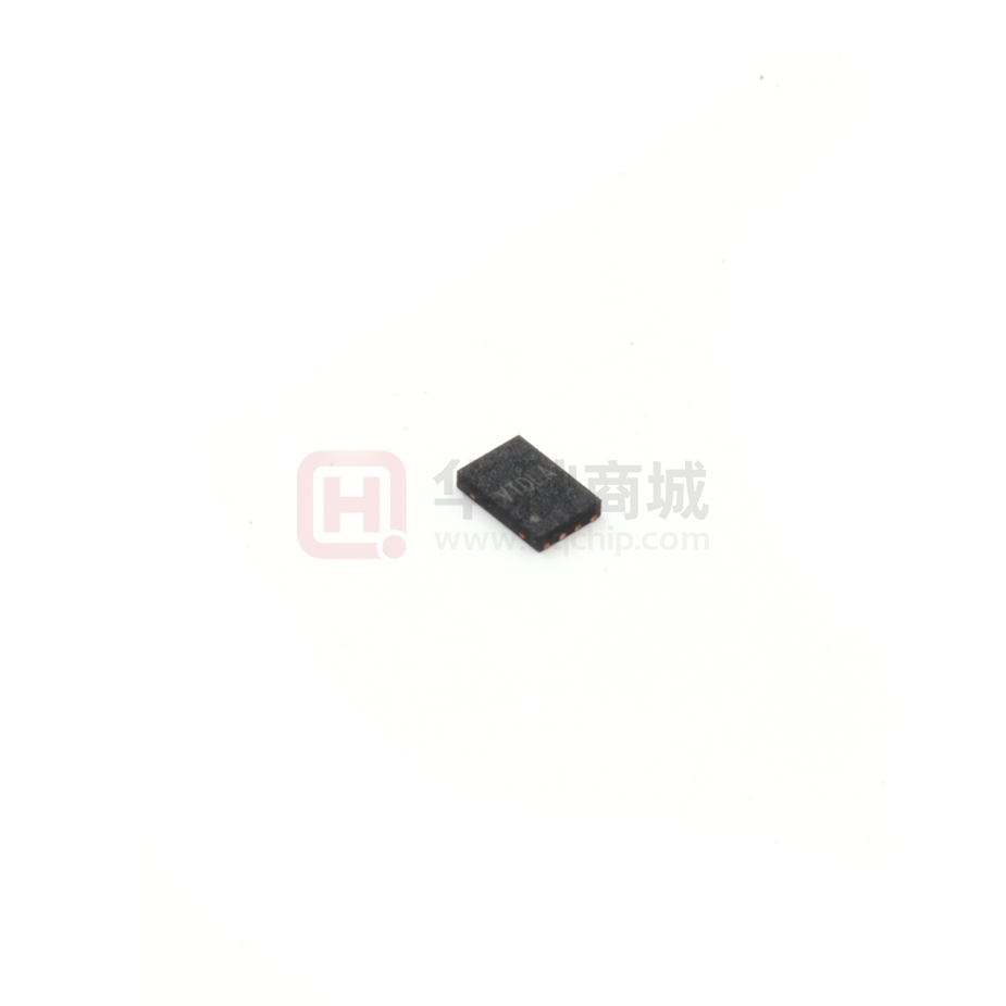
引脚分配:DFN2x3-8封装,包括输入引脚IN、输出引脚OUT、使能引脚EN、信号地SGND、反馈引脚FB、功率地PGND等。

参数特性: - 输入电压范围:2.3-5.0V - 可调输出电压:2.5V至5.5V - 峰值电流限制:3A - 伪恒频:1MHz - 低RDS(ON):在5.0V输出时,主开关/同步开关为70/100mohm

功能详解: - 具有输入欠压锁定、输出过压保护、负载断开等功能。 - 可通过连接反馈电阻Ru和Rf在OUT和FB之间来设置输出电压。

应用信息:适用于所有单节锂电或双节电池供电的产品,如MP3播放器、PDA和其他便携设备。

封装信息:紧凑的DFN2x3-8封装。
SY7088DGC 价格&库存

很抱歉,暂时无法提供与“SY7088DGC”相匹配的价格&库存,您可以联系我们找货

免费人工找货
SY7088DGC
  •  国内价格
  • 1+1.28700
  • 30+1.24200
  • 100+1.15200
  • 500+1.06200
  • 1000+1.01700

库存:479