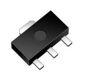
WL2855K
WL2855K
Low noise, Low Power Consumption, 12V
Input, 500mA, CMOS LDO
Http://www.sh-willsemi.com
Descriptions
The WL2855K series are high accuracy, low noise,
12V Input, 500mA, CMOS Linear regulator with high
ripple rejection. The devices offer a new level of cost
effective performance in cellular phones, laptop and
SOT-89-3L
notebook computers, and other portable devices.
The WL2855K has the fold-back maximum output
current which depends on the output voltage. So the
current limit functions both as a short circuit protection
and as an output current limiter.
The WL2855K regulators are available in standard
SOT-89-3L Package. Standard products are Pb-free
and Halogen-free.
Pin Configuration (Top View)
Features
Input Voltage Range
: 2.5V~12V
Output Voltage Range
:1.2V~5V
Output Current
:500mA
Fixed Voltage Accuracy
:±1%(Vo≥2.5V)
Quiescent current
:1uA
Dropout voltage
: 840mV@Vo=4V
2855 : Device code
Io=500mA
Recommend capacitor
Short-Circuit Protection
** : Voltage code
: ≥0.1uF
Y : Year Code
W : Week Code
Applications
Mobile Phone
Cellphones, radiophone, digital cameras
Bluetooth, wireless handsets
Others portable electronics device
For detail marking information, please see page 12.
Marking
Order Information
For detail order information, please see page 12.
Will Semiconductor Ltd.
1
Oct, 2019 – Rev 1.2
�WL2855K
Typical Application
Pin Description
SOT-89-3L
PIN
Symbol
Description
1
GND
Ground
2
VIN
Input
3
VOUT
Output
Recommend capacitor :≥0.1uF
Block Diagram
Will Semiconductor Ltd.
2
Oct, 2019 – Rev 1.2
�WL2855K
Absolute Maximum Ratings
Parameter
Value
Power Dissipation, PD@TA=25℃
1.5
W
VIN Range
-0.3~13.5
V
VOUT Range
-0.3~5.5
V
IOUT
Internally Limited
Lead Temperature Range
260
o
Storage Temperature Range
-55~150
o
Operating Junction Temperature Range
150
o
MSL
Level-3
ESD Ratings
Unit
mA
C
C
C
HBM
4000
V
MM
200
V
Recommend Operating Ratings
Parameter
Value
Unit
Operating Supply voltage
2.5~12
V
Operating Temperature Range
-40~85
Thermal Resistance, RθJA (SOT-89-3L)
77
Will Semiconductor Ltd.
3
C
o
C/W
o
Oct, 2019 – Rev 1.2
�WL2855K
Electronics Characteristics
(Ta=25oC, VIN=VOUT+1V, CIN=COUT=1μF, IOUT=1mA,unless otherwise noted)
Parameter
Symbol
Condition
VOUT≤2.5V
Output Voltage
VOUT
Input Voltage
VIN
Current Limit
ILIM
Dropout Voltage
VDROP
Line Regulation
△VLINE
Load Regulation
Min.
Typ.
Max.
Unit
-25
VOUT
+25
mV
0.99*
VOUT>2.5V
Vout
VOUT
2.5
VIN≥3.3V
1.01*
V
Vout
12
500
V
mA
VOUT=3.3V, IOUT=500mA
940
1200
mV
VOUT=4V, IOUT=500mA
840
1100
mV
VIN=VOUT+1~12V
1
5
mV
△VLoad
IOUT=1~500mA
30
50
mV
Quiescent Current
IQ
VIN=4V, IOUT=0
1
2.2
μA
Short Current
ISHORT
VOUT short to GND
Power Supply Rejection Rate
Output Noise Voltage
Will Semiconductor Ltd.
PSRR
eNO
Vo=3.3V, Io=10mA
Vo=3.3V, Io=30mA
4
180
mA
f=100Hz
70
dB
f=1kHz
50
dB
f=10kHz
25
dB
54
μVRMS
Oct, 2019 – Rev 1.2
�WL2855K
Typical characteristics (Ta=25oC, VIN=VOUT+1V, IOUT=1mA,CIN=COUT=1μF, unless otherwise noted)
VOUT=3.3V
VOUT=4.0V
VOUT=3.3V
Will Semiconductor Ltd.
5
Oct, 2019 – Rev 1.2
�WL2855K
VOUT=4.0V
Vdropout
VOUT=3.3V
Will Semiconductor Ltd.
VOUT=4.0V
6
Oct, 2019 – Rev 1.2
�WL2855K
VOUT=3.3V
Will Semiconductor Ltd.
VOUT=4.0V
7
Oct, 2019 – Rev 1.2
�WL2855K
1.Start up & Shut down
VOUT=3.3V
VIN=4.3V,COUT=1μF,IOUT=1mA
VIN=4.3V,COUT=1μF,IOUT=500mA
VOUT=4V
VIN=5V,COUT=1μF,IOUT=1mA
VIN=5V,COUT=1μF,IOUT=500mA
Will Semiconductor Ltd.
8
Oct, 2019 – Rev 1.2
�WL2855K
2.Load & Line Transient
VIN=4.3V,VOUT=3.3V,COUT=1μF,IOUT=1mA-40mA
VIN=4.3V,VOUT=3.3V,COUT=1μF,IOUT=50mA-100mA
VIN=5V,VOUT=4V,COUT=1μF,IOUT=1mA-40mA
VIN=5V,VOUT=4V,COUT=1μF,IOUT=50mA-100mA
VIN=4.3-5.3V,VOUT=3.3V,IOUT=10mA
Will Semiconductor Ltd.
VIN=5-6V,VOUT=4V,IOUT=10mA
9
Oct, 2019 – Rev 1.2
�WL2855K
PACKAGE OUTLINE DIMENSIONS
SOT-89-3L
D
A
E1
E
D1
L
b1
e
c
b
e1
SIDE VIEW
TOP VIEW
SIDE VIEW
Symbol
Dimensions in Millimeters
Min.
Typ.
Max.
A
1.40
1.50
1.60
b
0.32
0.42
0.52
b1
0.40
0.49
0.58
c
0.30
0.40
0.50
D
4.40
4.50
4.60
D1
1.60 Ref
E
2.30
2.45
2.60
E1
3.75
4.00
4.25
e
1.50 BSC
e1
3.00 BSC
L
1.05 Ref
Will Semiconductor Ltd.
10
Oct, 2019 – Rev 1.2
�TAPE AND REEL INFORMATION
Reel Dimensions
RD
Reel Dimensions
Tape Dimensions
W
P1
Quadrant Assignments For PIN1 Orientation In Tape
Q1
Q2
Q1
Q2
Q3
Q4
Q3
Q4
RD
Reel Dimension
W
Overall width of the carrier tape
P1
Pitch between successive cavity centers
Pin1
Pin1 Quadrant
Will Semiconductor Ltd.
User Direction of Feed
7inch
13inch
1 8mm
12mm
16mm
2mm
4mm
8mm
Q1
Q2
Q3
11
Q4
Oct, 2019 – Rev 1.2
�ORDER INFORMATION
Ordering No.
Vout
(V)
Package
Operating
Temperature
Marking
WL2855K18-3/TR
1.8
SOT-89-3L
-40~85℃
BJYW
WL2855K28-3/TR
2.8
SOT-89-3L
-40~85℃
CJYW
WL2855K30-3/TR
3.0
SOT-89-3L
-40~85℃
DAYW
WL2855K33-3/TR
3.3
SOT-89-3L
-40~85℃
DDYW
WL2855K37-3/TR
3.7
SOT-89-3L
-40~85℃
DHYW
WL2855K38-3/TR
3.8
SOT-89-3L
-40~85℃
DJYW
WL2855K40-3/TR
4.0
SOT-89-3L
-40~85℃
EAYW
WL2855K50-3/TR
5.0
SOT-89-3L
-40~85℃
FAYW
Will Semiconductor Ltd.
12
Shipping
Tape and Reel,
1000
Tape and Reel,
1000
Tape and Reel,
1000
Tape and Reel,
1000
Tape and Reel,
1000
Tape and Reel,
1000
Tape and Reel,
1000
Tape and Reel,
1000
Oct, 2019 – Rev 1.2
�
