WPE12VD3ULA
1-Line Low Capacitance Bi-directional TVS Diode
Description
Mechanical Characteristics
The WPE12VD3ULA is a 12V bi-directional TVS diode,
utilizing leading monolithic silicon technology to provide
fast re-sponse time and low ESD clamping voltage,
making this device an ideal solution for protecting voltage
sensitive high-speed data lines. The WPE12VD3ULA has
a low capaci-tance with a typical value at 1pF, and
complies with the IEC 61000-4-2 (ESD) with ±30kV air
and ±30kV contact discharge. It is assembled into a leadfree SOD-323 package. The small size, low capacitance
and high ESD surge protection make WPE12VD3ULA an
ideal choice to pro-tect cell phone, wireless systems, and
communication equipment.
•
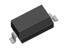
Package: SOD-323
•
•
Lead Finish: Matte Tin
Case Material: “Green” Molding Compound.
•
Moisture Sensitivity: Level 3 per J-STD-020
•
Terminal Connections: See Diagram Below
•
Marking Information: See Below
Features
•
350W peak pulse power (8/20μs)
•
Ultra low capacitance: 1pF typical
•
•
Ultra low leakage: nA level
Operating voltage: 12V
•
Low clamping voltage
•
Protects one power line or data line
•
Complies with following standards:
– IEC 61000-4-2 (ESD) immunity test
Air discharge: ±30kV
Contact discharge: ±30kV
– IEC61000-4-5 (Lightning) 12A (8/20μs)
RoHS Compliant
•
Dimensions and Pin Configuration
Applications
•
USB Ports
•
Smart Phones
•
Wireless Systems
•
Ethernet 10/100/1000 Base T
Marking Information
DC
R2
Ordering Information
1
Part Number
WPE12VD3ULA
Packaging
3000/Tape & Reel
Reel Size
7 inch
2
Circuit and Pin Schematic
V1.0_Aug,2018
-1-
www.wpmtek.com
�WPE12VD3ULA
1-Line Low Capacitance Bi-directional TVS Diode
Absolute Maximum Ratings (TA=25°C unless otherwise specified)
Parameter
Symbol
Value
Unit
Peak Pulse Power (8/20µs)
Ppk
350
W
Peak Pulse Current (8/20µs)
IPP
12
A
ESD per IEC 61000−4−2 (Air)
±30
VESD
ESD per IEC 61000−4−2 (Contact)
Operating Temperature Range
Storage Temperature Range
kV
±30
TJ
−55 to +125
°C
Tstg
−55 to +150
°C
Electrical Characteristics (TA=25°C unless otherwise specified)
Parameter
Reverse Working Voltage
Breakdown Voltage
Symbol
Min
Typ
VRWM
VBR
Max
Unit
12
V
13.3
Test Condition
V
IT = 1mA
Reverse Leakage Current
IR
0.2
μA
VRWM = 12V
Clamping Voltage
VC
18
V
IPP = 1A (8 x 20µs pulse)
Clamping Voltage
VC
29
V
IPP = 12A (8 x 20µs pulse)
Junction Capacitance
CJ
pF
VR = 0V, f = 1MHz
V1.0_Aug,2018
1
-2-
www.wpmtek.com
�WPE12VD3ULA
1-Line Low Capacitance Bi-directional TVS Diode
Typical Performance Characteristics (TA=25°C unless otherwise Specified)
Peak Power_Ppp(kW)
10
1
0.1
0.01
0.1
1
10
Pulse Duration_tp(μs)
Junction Capacitance vs. Reverse Voltage
Peak Pulse Power vs. Pulse Time
Clamping Voltage vs. Peak Pulse Current
Power Derating Curve
100
ESD Clamping Voltage
8 X 20μs Pulse Waveform
V1.0_Aug,2018
8 kV Contact per IEC61000−4−2
-3-
www.wpmtek.com
�WPE12VD3ULA
1-Line Low Capacitance Bi-directional TVS Diode
SOD-323 Package Outline Drawing
MILLIMETERS
NOM
SYM
MIN
A
0.800
--
1.100
A1
0.800
--
0.900
A2
0.000
--
0.100
b
0.250
--
0.400
c
0.080
--
0.177
D1
1.600
1.700
1.800
D
2.300
--
2.800
E
1.150
--
1.400
L
MAX
0.475REF
L1
0.100
--
0.500
Θ
0°
--
8°
Suggested Land Pattern
Unit:mm
V1.0_Aug,2018
-4-
www.wpmtek.com
�
很抱歉,暂时无法提供与“WPE12VD3ULA”相匹配的价格&库存,您可以联系我们找货
免费人工找货- 国内价格
- 10+0.44939
- 100+0.36126
- 300+0.31720
- 3000+0.26244
- 6000+0.23598
- 9000+0.22270