RTL2832U
k
e
t
l
a
e
R
L
IA
T
N
DVB-T COFDM DEMODULATOR+USB 2.0
E
ID
F
N
DATASHEET
(CONFIDENTIAL: Development Partners Only)
O
C
r
fo
L
4
V
Rev. 1.4
01 November 2010
Track ID: JATR-2265-11
Realtek Semiconductor Corp.
No. 2, Innovation Road II, Hsinchu Science Park, Hsinchu 300, Taiwan
Tel.: +886-3-578-0211. Fax: +886-3-577-6047
www.realtek.com
�RTL2832U
Datasheet
COPYRIGHT
©2010 Realtek Semiconductor Corp. All rights reserved. No part of this document may be reproduced,
transmitted, transcribed, stored in a retrieval system, or translated into any language in any form or by any
means without the written permission of Realtek Semiconductor Corp.
DISCLAIMER
Realtek provides this document “as is”, without warranty of any kind. Realtek may make improvements
and/or changes in this document or in the product described in this document at any time. This document
could include technical inaccuracies or typographical errors.
TRADEMARKS
k
e
t
l
a
Realtek is a trademark of Realtek Semiconductor Corporation. Other names mentioned in this document
are trademarks/registered trademarks of their respective owners.
e
R
USING THIS DOCUMENT
L
IA
This document is intended for the hardware and software engineer’s general information on the Realtek
RTL2832U.
T
N
Though every effort has been made to ensure that this document is current and accurate, more information
may have become available subsequent to the production of this guide.
REVISION HISTORY
E
ID
F
N
Revision
1.0
1.1
Release Date
2008/06/30
2009/02/06
1.2
2009/02/16
1.3
1.4
2009/06/29
2010/11/01
O
C
DVB-T COFDM Demodulator + USB 2.0
Summary
First release.
Corrected typing errors.
Revised ‘Connects a 12k ohm Resistor to ground’ to ‘Connects a 10k ohm
Resistor to ground’, in the ADC section of Table 1 Pin Descriptions, page 5.
Revised Figure 9, page 44.
Corrected minor typing errors.
Added Table 38 Crystal Conditions, page 43.
r
fo
L
4
V
ii
Track ID: JATR-2265-11
Rev. 1.4
�RTL2832U
Datasheet
Table of Contents
1.
GENERAL DESCRIPTION ..............................................................................................................................................1
2.
FEATURES .........................................................................................................................................................................2
3.
SYSTEM APPLICATIONS...............................................................................................................................................2
4.
BLOCK DIAGRAM ...........................................................................................................................................................3
5.
PIN ASSIGNMENTS .........................................................................................................................................................4
5.1.
k
e
t
GREEN PACKAGE AND VERSION IDENTIFICATION ........................................................................................................4
6.
PIN DESCRIPTIONS.........................................................................................................................................................5
7.
FUNCTIONAL DESCRIPTION.......................................................................................................................................7
7.1.
7.2.
7.3.
7.4.
7.5.
7.6.
7.7.
7.8.
7.9.
7.10.
7.11.
8.
ANALOG-TO-DIGITAL CONVERSION (ADC).................................................................................................................7
AUTOMATIC GAIN CONTROL (AGC)............................................................................................................................7
DIGITAL DOWN CONVERSION ......................................................................................................................................7
RESAMPLER .................................................................................................................................................................8
GUARD INTERVAL REMOVAL .......................................................................................................................................8
FAST FOURIER TRANSFORM (FFT)...............................................................................................................................8
SYNCHRONIZATION ......................................................................................................................................................8
CHANNEL ESTIMATION ................................................................................................................................................9
TRANSMISSION PARAMETER SIGNAL DECODER ...........................................................................................................9
EQUALIZATION ............................................................................................................................................................9
DE-INTERLEAVER, FEC DECODER, AND DESCRAMBLER .............................................................................................9
l
a
e
R
L
IA
T
N
TUNER INTERFACE......................................................................................................................................................10
E
ID
8.1.
AUTOMATIC GAIN CONTROL (AGC)..........................................................................................................................11
8.1.1. Register Name: loop_gain ....................................................................................................................................12
8.1.2. Register Name: if_agc_min/if_agc_max/rf_agc_min/rf_agc_max .......................................................................13
8.1.3. Register Name: Vtop.............................................................................................................................................13
8.1.4. Register Name: Krf...............................................................................................................................................14
8.1.5. Register Name: if_agc_val/rf_agc_val .................................................................................................................14
8.2.
ADC INPUT (TUNER OUTPUT) ...................................................................................................................................14
8.3.
TWO-WIRE INTERFACE BETWEEN THE TUNER AND THE RTL2832U .........................................................................15
8.4.
RTL2832U INTERNAL SWITCHING REGULATOR ........................................................................................................16
9.
F
N
O
C
REGISTER DESCRIPTIONS (GENERAL)..................................................................................................................17
9.1.
9.2.
9.3.
9.4.
9.5.
9.6.
9.7.
9.8.
9.9.
9.10.
9.11.
10.
L
4
V
ANALOG TO DIGITAL CONVERTER (ADC) .................................................................................................................17
DC CANCELLATION AND IQ COMPENSATION ............................................................................................................18
DIGITAL DOWN CONVERSION (DDC) ........................................................................................................................19
RESAMPLER ...............................................................................................................................................................20
CO-CHANNEL INTERFERENCE REJECTION ..................................................................................................................21
IMPULSE NOISE CANCELLATION ................................................................................................................................21
DIGITAL AUTOMATIC GAIN CONTROL (DAGC) ........................................................................................................22
FFT MODE DETECTION ..............................................................................................................................................22
TIMING RECOVERY/CARRIER RECOVERY ..................................................................................................................23
CRYSTAL....................................................................................................................................................................24
PID FILTER ................................................................................................................................................................24
r
fo
REGISTER DESCRIPTIONS (8051 SYSTEM) .......................................................................................................27
10.1.
DEMODULATOR CONTROL REGISTER (DEMOD_CTL, 0000H) .................................................................................29
10.2.
GPIO RELATED REGISTERS (0001H~0008H) .............................................................................................................29
10.2.1.
GPIO Output Value Register (GPO, 0001h) ...................................................................................................30
DVB-T COFDM Demodulator + USB 2.0
iii
Track ID: JATR-2265-11
Rev. 1.4
�RTL2832U
Datasheet
10.2.2.
GPIO Input Value Register (GPI, 0002h)........................................................................................................30
10.2.3.
GPIO Output Enable Register (GPOE, 0003h) ...............................................................................................31
10.2.4.
GPIO Direction Control Register (GPD, 0004h) ............................................................................................31
10.2.5.
PAD Configuration Register for GPIO0~3 (GP_CFG0, 0007h).....................................................................32
10.2.6.
PAD Configuration Register for GPIO4 (GP_CFG1, 0008h).........................................................................32
10.3.
I2C MASTER CONTROL REGISTERS (0040H-0053H) ...................................................................................................33
10.3.1.
I2C Clock Register (I2CCR, 0040h-0043h)......................................................................................................33
10.3.2.
I2C Master Control Register (I2CMCR, 0044h-0047h)...................................................................................33
10.3.3.
I2C Master SCL Timing Register (I2CMSTR, 0048h-004Bh) ..........................................................................35
10.3.4.
I2C Master Status Register (I2CMSR, 004Ch-004Fh) .....................................................................................35
10.3.5.
I2C Master FIFO Register (I2CMFR, 0050h-0053h) ......................................................................................36
11.
k
e
t
REGISTER DESCRIPTIONS (USB INTERFACE) ................................................................................................36
11.1.
INTRODUCTION ..........................................................................................................................................................36
11.2.
VENDOR COMMANDS .................................................................................................................................................36
11.3.
SIE CONTROL REGISTER ............................................................................................................................................38
11.4.
USB SYSTEM CONTROL REGISTER (USB_SYSCTL, 0000H) ....................................................................................39
11.4.1.
Endpoint A Configuration Register (USB_EPA_CFG, 0144h) .......................................................................39
11.4.2.
Endpoint A Control Register (USB_EPA_CTL, 0148h) ..................................................................................40
11.4.3.
Endpoint A Max Packet Size Register (USB_EPA_MAXPKT, 0158h) ............................................................40
11.4.4.
Endpoint A FIFO Configuration Register (USB_EPA_FIFO_CFG, 0160h) ..................................................40
12.
12.1.
12.2.
12.3.
12.4.
l
a
e
R
L
IA
CHARACTERISTICS.................................................................................................................................................41
ABSOLUTE MAXIMUM RATINGS ................................................................................................................................41
DC CHARACTERISTICS ...............................................................................................................................................41
AC CHARACTERISTICS ...............................................................................................................................................42
CRYSTAL CONDITIONS ...............................................................................................................................................43
T
N
E
ID
13.
APPLICATION CIRCUITS .......................................................................................................................................44
14.
MECHANICAL DIMENSIONS.................................................................................................................................45
14.1.
15.
MECHANICAL DIMENSIONS NOTES ............................................................................................................................46
F
N
ORDERING INFORMATION ...................................................................................................................................47
O
C
DVB-T COFDM Demodulator + USB 2.0
r
fo
L
4
V
iv
Track ID: JATR-2265-11
Rev. 1.4
�RTL2832U
Datasheet
List of Tables
TABLE 1.
TABLE 2.
TABLE 3.
TABLE 4.
TABLE 5.
TABLE 6.
TABLE 7.
TABLE 8.
TABLE 9.
TABLE 10.
TABLE 11.
TABLE 12.
TABLE 13.
TABLE 14.
TABLE 15.
TABLE 16.
TABLE 17.
TABLE 18.
TABLE 19.
TABLE 20.
TABLE 21.
TABLE 22.
TABLE 23.
TABLE 24.
TABLE 25.
TABLE 26.
TABLE 27.
TABLE 28.
TABLE 29.
TABLE 30.
TABLE 31.
TABLE 32.
TABLE 33.
TABLE 34.
TABLE 35.
TABLE 36.
TABLE 37.
TABLE 38.
TABLE 39.
PIN DESCRIPTIONS ........................................................................................................................................................5
AAGC REGISTER TABLE ............................................................................................................................................12
I2C REPEATER REGISTER TABLE .................................................................................................................................15
ADC REGISTERS .........................................................................................................................................................17
DC CANCELLATION REGISTERS ..................................................................................................................................18
DIGITAL DOWN CONVERSION (DDC) .........................................................................................................................20
RESAMPLER ................................................................................................................................................................20
CO-CHANNEL INTERFERENCE REJECTION...................................................................................................................21
IMPULSE NOISE CANCELLATION .................................................................................................................................21
DAGC REGISTERS .....................................................................................................................................................22
FTT MODE DETECTION..............................................................................................................................................22
TIMING RECOVERY/CARRIER RECOVERY ..................................................................................................................24
PID FILTER ................................................................................................................................................................25
SYSTEM REGISTER DESCRIPTIONS .............................................................................................................................27
DEMODULATOR CONTROL REGISTER (DEMOD_CTL, 0000H) .................................................................................29
GPIO OUTPUT VALUE REGISTER (GPO, 0001H) .......................................................................................................30
GPIO INPUT VALUE REGISTER (GPI, 0002H) ............................................................................................................30
GPIO OUTPUT ENABLE REGISTER (GPOE, 0003H) ...................................................................................................31
GPIO DIRECTION CONTROL REGISTER (GPD, 0004H)...............................................................................................31
PAD CONFIGURATION REGISTER FOR GPIO0~3 (GP_CFG0, 0007H) .......................................................................32
PAD CONFIGURATION REGISTER FOR GPIO4 (GP_CFG1, 0008H)............................................................................32
I2C CLOCK REGISTER (I2CCR, 0040H-0043H)...........................................................................................................33
I2C MASTER CONTROL REGISTER (I2CMCR, 0044H-0047H) ....................................................................................33
I2C MASTER SCL TIMING REGISTER (I2CMSTR, 0048H-004BH) .............................................................................35
I2C MASTER STATUS REGISTER (I2CMSR, 004CH-004FH) .......................................................................................35
I2C MASTER FIFO REGISTER (I2CMFR, 0050H-0053H)............................................................................................36
VENDOR COMMANDS .................................................................................................................................................36
DEFINITION OF ‘WINDEX’...........................................................................................................................................37
SIE CONTROL REGISTER ............................................................................................................................................38
USB SYSTEM CONTROL REGISTER (USB_SYSCTL, 0000H) ....................................................................................39
ENDPOINT A CONFIGURATION REGISTER (USB_EPA_CFG, 0144H) ........................................................................39
ENDPOINT A CONTROL REGISTER (USB_EPA_CTL, 0148H)....................................................................................40
ENDPOINT A MAX PACKET SIZE REGISTER (USB_EPA_MAXPKT, 0158H) ............................................................40
ENDPOINT A FIFO CONFIGURATION REGISTER .........................................................................................................40
ABSOLUTE MAXIMUM RATINGS ................................................................................................................................41
DC CHARACTERISTICS ...............................................................................................................................................41
TWO-WIRE INTERFACE TIMING .................................................................................................................................42
CRYSTAL CONDITIONS ...............................................................................................................................................43
ORDERING INFORMATION ..........................................................................................................................................47
k
e
t
l
a
e
R
O
C
DVB-T COFDM Demodulator + USB 2.0
T
N
E
ID
F
N
r
fo
L
IA
L
4
V
v
Track ID: JATR-2265-11
Rev. 1.4
�RTL2832U
Datasheet
List of Figures
FIGURE 1.
FIGURE 2.
FIGURE 3.
FIGURE 4.
FIGURE 5.
FIGURE 6.
FIGURE 7.
FIGURE 8.
FIGURE 9.
BLOCK DIAGRAM ........................................................................................................................................................3
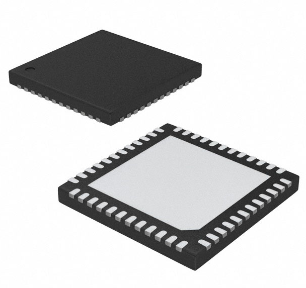
PIN ASSIGNMENTS (48-PIN QFN) ................................................................................................................................4
IF OR ZERO-IF TUNER INTERFACE.............................................................................................................................10
DELAYED AGC .........................................................................................................................................................11
TWO-WIRE INTERFACE BETWEEN THE TUNER AND RTL2832U ................................................................................15
INTERNAL SWITCHING REGULATOR LAYOUT ............................................................................................................16
PID FILTER FUNCTION OF THE RTL2832U................................................................................................................24
TWO-WIRE INTERFACE TIMING DIAGRAM ................................................................................................................42
APPLICATION CIRCUITS .............................................................................................................................................44
k
e
t
l
a
e
R
O
C
DVB-T COFDM Demodulator + USB 2.0
T
N
E
ID
F
N
r
fo
L
IA
L
4
V
vi
Track ID: JATR-2265-11
Rev. 1.4
�RTL2832U
Datasheet
1.
General Description
The RTL2832U is a high-performance DVB-T COFDM demodulator that supports a USB 2.0 interface.
The RTL2832U complies with NorDig Unified 1.0.3, D-Book 5.0, and EN300 744 (ETSI Specification).
It supports 2K or 8K mode with 6, 7, and 8MHz bandwidth. Modulation parameters, e.g., code rate, and
guard interval, are automatically detected.
k
e
t
The RTL2832U supports tuners at IF (Intermediate Frequency, 36.125MHz), low-IF (4.57MHz), or
Zero-IF output using a 28.8MHz crystal. Embedded with an advanced ADC (Analog-to-Digital
Converter), the RTL2832U features high stability in portable reception.
l
a
L
IA
The state-of-the-art RTL2832U features Realtek proprietary algorithms (patent-pending), including
superior channel estimation, co-channel interface rejection, long echo channel reception, and impulse
noise cancellation, and provides an ideal solution for a wide range of applications for PC-TV, such as
USB dongle and MiniCard/USB, and embedded system via USB interface.
e
R
E
ID
F
N
O
C
DVB-T COFDM Demodulator + USB 2.0
T
N
r
fo
L
4
V
1
Track ID: JATR-2265-11
Rev. 1.4
�RTL2832U
Datasheet
2.
Features
COFDM complying with Nordig Unified
1.0.3, D-book 5.0, and ETSI 300-744
Delayed AGC with programmable
Take-Over Point (TOP)
Supports multiple IF frequencies (4.57MHz
or 36.167MHz) and spectrum inversion
7-bit ADC for RF signals level measurement
Hardware MPEG-2 PID filters
Infra-red port for remote control and
wake-up, protocols supported are
Supports Zero-IF input
Single low-cost crystal for clock generation
(±100ppm)
l
a
e
R
Impulse noise cancellation circuits
Automatic carrier recovery over a wide
range offset (±800KHz)
3.
k
e
t
Automatic transmission mode and guard
interval detection
System Applications
Portable DTV device
USB dongle
MiniCard
DVB-T COFDM Demodulator + USB 2.0
NEC, Sony, SIRC, RC-5 protocol
r
fo
L
IA
Eight general purpose I/O ports
USB 2.0 Interface
T
N
E
ID
F
N
O
C
Microsoft RC6 protocol
Superior performance with pre/post/long
echo profiles
Embedded adjacent and co-channel
interference rejection circuit
Supports USB Full/High speed
Configurable vendor information via
external EEPROM
Passes USB-IF certification
Signal 3.3V external power is required
L
4
V
2
48-pin QFN (6x6 mm2) Green Package
Track ID: JATR-2265-11
Rev. 1.4
�RTL2832U
Datasheet
4.
Block Diagram
IF to Baseband
Sampling Clock
28.8 MHz
Timing Error
LPF
I
90
ADC
Resampler
k
e
t
Q
LPF
RF AGC
AGC
Synchroniza
-tions
FFT
Frequency Error
l
a
IF AGC
USB
MPEG 2
e
R
Figure 1.
DVB-T COFDM Demodulator + USB 2.0
r
fo
Channel
Estimation/
Equalizer
L
IA
De-Mapper
T
N
Block Diagram
E
ID
F
N
O
C
Channel
Decoding &
De-Interleaver
MPEG 2
PID
Filter
L
4
V
3
Track ID: JATR-2265-11
Rev. 1.4
�RTL2832U
Datasheet
VDDA
VDDA33
UVDDA
HSDM
HSDP
SEGND
IRRC
GPIO0
Pin Assignments
k
e
t
48
47
46
45
44
43
42
41
40
39
38
37
R12K
VDDA
VCMI
GNDA
5.
l
a
e
R
L
IA
T
N
E
ID
O
C
AGC_IF
VDD3
AGC_RF
I2C_SCLT
I2C_SDAT
I2C_SCL
I2C_SDA
VDD1
GPIO7
GPIO6
FB
SW_VOUT1
13
14
15
16
17
18
19
20
21
22
23
24
F
N
r
fo
Figure 2.
L
4
V
Pin Assignments (48-Pin QFN)
5.1. Green Package and Version Identification
Green package is indicated by a ‘G’ in the location marked ‘T’ in Figure 2. The version number is shown
in the location marked ‘V’.
DVB-T COFDM Demodulator + USB 2.0
4
Track ID: JATR-2265-11
Rev. 1.4
�RTL2832U
Datasheet
6.
Pin Descriptions
The following signal type codes are used in the tables:
I: Input
I/OD: Bi-Directional, Output Open-Drain
O: Output
Tri: Tri-State Output
k
e
t
OD: Open-Drain Output
PS: Power Supply
I/O: Bi-Directional
GND: Ground
l
a
Table 1.
Name
Pin number
Pin Descriptions
Function
e
R
12, 20, 28, 34
VDD3
14, 33
VDDA33
43
VDDA
44, 47
Analog Front End Power Supplies
GNDA
3, 45
Analog Front End Ground
O
C
XO
VDDPLL
GNDPLL
TP_CKO
Digital Core Power Supplies
PS (1.2V)
T
N
Digital I/O Power Supplies
Analog Front End Power Supply
E
ID
F
N
XI
L
IA
Power and Ground
VDD1
Type
Oscillator and PLL
PS (3.3V)
PS (3.3V)
PS (1.2V)
GND
11
Crystal Oscillator Input
I
10
Crystal Oscillator Output
O
7
PLL Power Supply
8
PLL Ground
9
ADC Test Pin for Clock Input
VIP
1
VIN
2
VQP
4
V
r
fo
VQN
4L
ADC
PS (1.2V)
GND
I/O
Differential Analog Input – Positive (I Path)
I
Differential Analog Input – Negative (I Path)
I
Differential Analog Input – Positive (Q Path)
I
5
Differential Analog Input – negative (Q Path)
I
R12K
48
Connects a 10k ohm Resistor to Ground
I
VCMI
46
Reference Voltage for ADC AC-Coupling
I
DVB-T COFDM Demodulator + USB 2.0
5
Track ID: JATR-2265-11
Rev. 1.4
�RTL2832U
Datasheet
Name
Pin number
VINR
6
Function
Type
Low Speed 7-bit ADC Single-Ended Input
I
USB Interface
HSDP
40
USB D+ Signal
I/O
HSDM
41
USB D- Signal
I/O
UVDDA
42
USB 1.2V Analog Power Supply
SEGND
39
Reference Ground
PS (1.2V)
k
e
t
GND
Host Interface
I2C_SCL
18
I2C Interface Clock Output Pin (5 Voltage Tolerance)
I2C_SDA
19
I2C Interface Bi-Directional Data Pin (5 Voltage Tolerance)
I2C_SCLT
16
Output SCLK Signal (5 Voltage Tolerance) for Tuner Control
I2C_SDAT
17
Output SDAT Signal (5 Voltage Tolerance) for Tuner Control
AGC_IF
13
Control Signal for IF AGC (5 Voltage Tolerance)
AGC_RF
15
Control Signal for RF AGC (5 Voltage Tolerance)
M_ERR
35
MPEG Error Output
l
a
e
R
E
ID
I/OD
OD
L
IA
T
N
GPIO Interface and IR
OD
I/OD
OD
OD
O
IRRC
38
IR Signal Input
GPIO[0]
37
General Purpose I/O Pin-0
32
General Purpose I/O Pin-1
31
General Purpose I/O Pin-2
Tri
36
General Purpose I/O Pin-3
Tri
30
General Purpose I/O Pin-4
Tri
29
General Purpose I/O Pin-5
GPIO[6]
22
General Purpose I/O Pin-6
GPIO[7]
21
General Purpose I/O Pin-7
F
N
GPIO[1]
GPIO[2]
O
C
GPIO[3]
GPIO[4]
GPIO[5]
4L
Tri
Tri
Tri
V
r
o
f
I
Tri
Tri
Internal 3.3V to 1.2V Switching Regulator
ENSWREG
27
0V: Turn off switching regulator
I
3.3V: Turn on switching regulator (Tie high internally)
SW_VDD3
26, 25
REG_OUT
24
1.2V Power Output
O
FB
23
Regulated Feedback Voltage
I
DVB-T COFDM Demodulator + USB 2.0
3.3V Power Input
PS (3.3V)
6
Track ID: JATR-2265-11
Rev. 1.4
�RTL2832U
Datasheet
7.
Functional Description
The block diagram of the RTL2832U DVB-T demodulator is shown in Figure 1, page 3. The RTL2832U
accepts IF or Zero IF input signals with the analog signal sampled by the internal ADC. The sampled data
stream is then processed by OFDM demodulation. After decoding by an on-chip FEC (Viterbi and
Reed-Solomon decoder) the USB 2.0 interface outputs packets with transport stream data.
k
e
t
A detailed description of each block is given in this section.
l
a
7.1. Analog-to-Digital Conversion (ADC)
The internal A/D converter can accept tuner output with various bandwidths (6, 7, 8MHz), different IF
frequencies (4.57M or 36.167M,), Zero IF (I & Q channel) input and can perform spectrum reversion.
e
R
L
IA
Using a sampling clock generated by the internal PLL with a 28.8MHz clock source, the RTL2832U
demodulates the received TV signal.
T
N
E
ID
7.2. Automatic Gain Control (AGC)
F
N
The AGC circuit is used to adjust received signal strength to a moderate level for the ADC. This module
supports two output paths, and both are sigma-delta modulated signals. The output signals need additional
RC LPFs (Low-Pass Filters) before feeding to IF and RF VGA in the tuner The delayed AGC algorithm
is described in section 8.1 Automatic Gain Control (AGC), page 11.
O
C
7.3. Digital Down Conversion
r
fo
L
4
V
The RTL2832U uses IF or Zero-IF sampling to process received signals. The Digital Down Conversion
(DDC) circuit converts the sampled IF signal to a complex base-band signal for further processing. The
down conversion frequency and low-pass filter can be programmed according to different IF frequency,
sampling rates, and signal bandwidth.
DVB-T COFDM Demodulator + USB 2.0
7
Track ID: JATR-2265-11
Rev. 1.4
�RTL2832U
Datasheet
7.4. Resampler
The Resampler circuit changes the received signal from a fixed ADC sampling rate to an Orthogonal
Frequency Division Multiplexing (OFDM) sampling rate according to the signal bandwidth. The
conversion ratio can be programmed via a register setting.
k
e
t
7.5. Guard Interval Removal
In time domain modulation, there is a guard interval inserted between two Orthogonal Frequency
Division Multiplexing (OFDM) signals. It is necessary to remove the guard interval before Fast Fourier
Transform (FFT) processing. This module is used to moderate the OFDM symbol boundary for FFT
according to the results of synchronization.
l
a
e
R
7.6. Fast Fourier Transform (FFT)
L
IA
T
N
E
ID
The Fast Fourier Transform (FFT) circuit converts a received time domain signal to a frequency domain
signal. Based on the ETSI 300-744 definition, FFT output contains continuous pilots, scattered pilots,
Transmission Parameter Signal (TPS), and data signal. These signals can be used for synchronization,
channel estimation, and data decision in further processing.
F
N
O
C
7.7. Synchronization
L
4
V
The RTL2832U can measure and compensate for a large range of sampling frequency offsets and carrier
frequency offsets before making a data decision. A moderate symbol boundary is utilized to avoid InterSymbol Interference (ISI).
DVB-T COFDM Demodulator + USB 2.0
r
fo
8
Track ID: JATR-2265-11
Rev. 1.4
�RTL2832U
Datasheet
7.8. Channel Estimation
A channel estimation circuit is used to estimate the channel condition of received signals. The estimated
channel response can be used for equalization, and is updated symbol by symbol to support mobile
channel variations.
k
e
t
7.9. Transmission Parameter Signal Decoder
This module is used to decode and determine Transmission Parameter Signal (TPS) bits. The TPS carriers
contain parameters for demodulation. These parameters are protected by Bose, Ray-Chaudhuri,
Hocquenghem (BCH) encoding. After decoding, the RTL2832U demodulator further processes the
decoded information. Parameters such as transmission mode, guard interval value, code rate etc, can be
pre-set by registers to overwrite the result of TPS decoding.
l
a
e
R
7.10. Equalization
L
IA
T
N
E
ID
To handle various channel conditions, the equalization circuit compensates for the signal degradation
caused by different multi-path channel profiles. The data bit is detected based on the equalization output.
F
N
O
C
7.11. De-Interleaver, FEC Decoder, and Descrambler
L
4
V
In accordance with ETSI 300-744, the RTL2832U uses a de-interleaver to re-order the decision data bit to
the correct sequence. The Forward Error Correction (FEC) decoder circuit detects and corrects error bits
in the received sequence. The descrambler recovers the output of the decoder to a standard Transport
Stream (TS) sequence.
DVB-T COFDM Demodulator + USB 2.0
r
fo
9
Track ID: JATR-2265-11
Rev. 1.4
�RTL2832U
Datasheet
8.
Tuner Interface
There are three interfaces (AGC, ADC input, two-wire serial interface) between the tuner and the
demodulator.
k
e
t
l
a
e
R
O
C
r
fo
Figure 3.
DVB-T COFDM Demodulator + USB 2.0
T
N
E
ID
F
N
L
IA
L
4
V
IF or Zero-IF Tuner Interface
10
Track ID: JATR-2265-11
Rev. 1.4
�RTL2832U
Datasheet
8.1. Automatic Gain Control (AGC)
In the RTL2832U, the RF_AGC and IF_AGC pins control the Radio Frequency (RF) and Intermediate
Frequency (IF) VGA gain of the tuner. In some applications, the RTL2832U only controls IF VGA, and
the tuner controls RF VGA. In some tuners, only the RF AGC is needed. The RTL2832U uses delayed
AGC to control RF and IF AGC. Gain distribution for RF and IF VGA is adjusted by registers ‘vtop’ and
‘krf’. The delayed AGC method is shown in Figure 4. RTL2832U has three vtop and four krf register
values to be programmed by user.
k
e
t
When the input power of the RF tuner is weak, RF VGA gain is kept to the maximum for better tuner
performance. When the input power is strong enough, RF VGA starts to decrease its gain to avoid the
non-linearity effect of the following block (IF VGA). The point where RF VGA starts to decrease gain
value is vtop (the ‘take-over point’). The ratio for RF VGA gain decrease is set by register krf. The
optimal values of registers vtop and krf depend on the tuner used.
l
a
e
R
L
IA
Pins RF_AGC and IF_AGC are sigma-delta DAC output. An external Resistor/Capacitor (RC) low-pass
filter and pull-high resister should be placed on the PCB board to generate a quasi-DC control voltage to
the tuner as shown in Figure 3, page 10.
E
ID
F
N
O
C
r
fo
Figure 4.
DVB-T COFDM Demodulator + USB 2.0
T
N
L
4
V
Delayed AGC
11
Track ID: JATR-2265-11
Rev. 1.4
�RTL2832U
Datasheet
8.1.1.
Register Name: loop_gain
Analog Automatic Gain Control (AAGC) loop gain is set by register loop_gain2 and
loop_gain2. Register loop_gain2 can be set to 0~26. The value depends on the tuner. The
recommended value is 20 (dec). A larger loop_gain value would get a slower AAGC locking time, but
more stable AAGC control voltage. There are another loop_gain1 and loop_gain3 for special cases: use
loop_gain1 for aagc unlock, and use loop_gain3 for existing interference.
Table 2.
Offset
Bits
{LSB, MSB}
Used
Register Name
Page
polar_rf_agc
0
0x0E
polar_if_agc
0
0x0E
loop_gain2
1
0x04
1
0x04
en_rf_agc
1
0x04
en_if_agc
1
Default
(Hex)
[1]
RW
0
[0]
RW
0
[4:1]
RW
0
[5]
RW
0
Description
Inverse the AGC_RF Sigma-Delta Pin
0: Normal
RW
1
1: Inverse
L
IA
Inverse the AGC_IF Sigma-Delta Pin
0: Normal
1: Inverse
AGC Loop Gain (Bit0~Bit3) for AAGC Lock
T
N
Hold AAGC Value (Open AAGC Loop)
0: Disable
E
ID
[6]
F
N
O
C
RW
l
a
e
R
aagc_hold
k
e
t
AAGC Register Table
1: Enable
Enable RF AGC Loop
1: Enable
0: Disable
Enable IF AGC Loop
0x04
[7]
RW
1
0x05
[7]
RW
1
AAGC Loop Gain (Bit4) for AAGC Lock
0xC7
[5:1]
RW
C
AAGC Loop Gain for AAGC Unlock
0xC8
[4:0]
RW
RW
loop_gain2
1
loop_gain1
1
loop_gain3
1
vtop1
1
0x06
[5:0]
vtop2
1
0xC9
vtop3
1
0xCA
krf1
1
0xCB
krf2
1
0x07
r
fo
krf3
1
krf4
if_agc_min
1: Enable
0: Disable
L
4
V
1A
AAGC Loop Gain for Existing Interference
10
u(6,5f) Set Take-Over Point1
30
u(6,5f) Set Take-Over Point2
28
u(6,5f) Set Take-Over Point3
[5:0]
RW
[5:0]
RW
[7:0]
RW
2
u(8,4f) Set RF AGC Gain Degrade Ratio1
[7:0]
RW
F
u(8,4f) Set RF AGC Gain Degrade Ratio2
0xCD
[7:0]
RW
20
u(8,4f) Set RF AGC Gain Degrade Ratio3
1
0xCE
[7:0]
RW
30
u(8,4f) Set RF AGC Gain Degrade Ratio4
1
0x08
[7:0]
RW
80
s(8,7f) Set IF AAGC Minimum Gain
DVB-T COFDM Demodulator + USB 2.0
12
Track ID: JATR-2265-11
Rev. 1.4
�RTL2832U
Datasheet
Offset
Bits
{LSB, MSB}
Used
1
0x09
[7:0]
RW
7F
s(8,7f) Set IF AAGC Maximum Gain
rf_agc_min
1
0x0A
[7:0]
RW
80
s(8,7f) Set RF AAGC Minimum Gain
rf_agc_max
1
0x0B
[7:0]
RW
7F
s(8,7f) Set RF AAGC Maximum Gain
if_agc_val
3
{59,5A}
[13:0]
R
-
rf_agc_val
3
{5B,5C}
[13:0]
R
-
aagc_lock
3
0x50
[0]
R
-
Register Name
Page
if_agc_max
8.1.2.
RW
Default
(Hex)
Description
s(14, 13f) IF AAGC Value
l
a
k
e
t
s(14, 13f) RF AAGC Value
AAGC Lock
Register Name: if_agc_min/if_agc_max/rf_agc_min/rf_agc_max
Format: s(8,7f)
e
R
L
IA
These registers limit the minimum and maximum value of RF/IF AGC. They are in 8-bit two’s
complement format. The maximum value 127 (dec) means maximum output voltage.
T
N
For example, if we want to limit RF minimum/maximum, AGC output voltage would be 10%/90% of
pull-high voltage.
E
ID
rf_agc_min=floor (10%*255-128)=-103 (dec)
rf_agc_max=floor (90%*255-128)=101 (dec)
F
N
O
C
8.1.3.
Register Name: Vtop
Format: u(6,6f)
L
4
V
The take-over point of RF VGA is set by register vtop. There are two special cases shown below. The
optimal value depends on the tuner.
r
fo
vtop=0 (dec) Æ RF gain is always set on maximum value
vtop=63 (dec)Æ RF gain does not delay
For example, if we want to degrade RF VGA gain when IF VGA control voltage is smaller than 0.5*Vdd:
vtop=floor (63*0.5)=31 (dec)
DVB-T COFDM Demodulator + USB 2.0
13
Track ID: JATR-2265-11
Rev. 1.4
�RTL2832U
Datasheet
8.1.4.
Register Name: Krf
Format: u(6,2f)
The gain degrade ratio between the RF and IF AGC when input power exceeds the RF take-over point is
set by register Krf. A larger krf means the RF Gain degrade ratio is larger. This means an equal gain
degrade ratio between the RF and the IF AGC. If we want RF gain to degrade quickly when input power
is larger than the take-over point, krf should be set to a larger value. If only IF AGC is controlled by the
RTL2832U, registers vtop and krf are not used.
8.1.5.
k
e
t
Register Name: if_agc_val/rf_agc_val
l
a
Format: s(14,13f)
L
IA
The RF AAGC value and IF AAGC value are read from registers if_agc_val/rf_agc_val. They are in
14-bit two’s complement format. The minimum value is –8192 and maximum value is 8191. When
rf/if_agc_val is set to the maximum value, it means the RF/IF AGC pin output is at the maximum control
voltage. The real RF input power can be mapped from if_agc_val/rf_agc_val. The mapping can be to a
table or an equation. Note that different vtop and krf settings map different tables and equations.
e
R
T
N
E
ID
8.2. ADC Input (Tuner Output)
F
N
Tuner IF or Zero IF output is AC coupled to the RTL2832U differential ADC input. An external AC
coupling capacitor is required. The schematic is shown in Figure 3, page 10.
O
C
DVB-T COFDM Demodulator + USB 2.0
r
fo
L
4
V
14
Track ID: JATR-2265-11
Rev. 1.4
�RTL2832U
Datasheet
8.3. Two-Wire Interface Between the Tuner and the RTL2832U
l
a
e
R
Figure 5.
k
e
t
L
IA
Two-Wire Interface between the Tuner and RTL2832U
T
N
E
ID
The RTL2832U supports an I2C repeater to prevent tuner interference from the two-wire interface. In
normal situations the tuner cannot hear any command sent via the two-wire interface. We need to turn on
the I2C repeater (set register IIC_repeat=1) in order to send a command to the tuner. The command will
be heard by the tuner and the RTL2832U at the same time. The Tuner and RTL2832U can distinguish the
origin of the command by the I2C address. On the PCB, pin I2C_SDAT/I2C_SCLT should be connected
to pull-high resisters (10k ohm) to pull-high the two-wire bus.
O
C
F
N
Register Name
IIC_repeat
Page
1
Table 3.
I2C Repeater Register Table
Offset{MSB,LSB} Bits Used
0x01
4L
RW
V
r
fo
[3]
RW
Default (Hex) Description
0
I2C Repeater for Tuner
1: Enable
0: Disable
Note 1: IIC_repeat should be set to 1 before sending a command to the tuner.
Note2: IIC_repeat is not automatically set to 0 after receiving a ‘STOP’ command.
DVB-T COFDM Demodulator + USB 2.0
15
Track ID: JATR-2265-11
Rev. 1.4
�RTL2832U
Datasheet
8.4. RTL2832U Internal Switching Regulator
The RTL2832U integrates a switching regulator with input voltage 3.3V to output voltage 1.2V. Figure 6
shows the application circuit.
The ENSWREG pin default power is 3.3V. Applying 0V turns off the switching regulator.
k
e
t
l
a
e
R
O
C
DVB-T COFDM Demodulator + USB 2.0
T
N
E
ID
F
N
Figure 6.
L
IA
L
4
V
Internal Switching Regulator Layout
r
fo
16
Track ID: JATR-2265-11
Rev. 1.4
�RTL2832U
Datasheet
9.
Register Descriptions (General)
9.1. Analog to Digital Converter (ADC)
The RTL2832U can receive IF or Zero-IF signals from the tuner. The following registers set IF or
Zero-IF mode.
k
e
t
IF signal mode
•
AD_EN_reg1 set 1
•
AD_EN_reg0 set 0
•
en_bbin set 0
l
a
Zero-IF signal mode
e
R
•
AD_EN_reg1 set 1
•
AD_EN_reg0 set 1
•
en_bbin set 1
Offset
Register Name
Page
AD_EN_reg1
0
AD_EN_reg
0
en_bbin
1
0xB1
opt_adc_iq
0
0x06
ADC Registers
Default
Bits Used
RW
0x08
[6]
RW
0
0x08
[7]
RW
0
F
N
O
C
T
N
E
ID
Table 4.
{MSB,LSB}
DVB-T COFDM Demodulator + USB 2.0
L
IA
(Hex)
RW
[5:4]
RW
17
1: Enable ADC_Q
0: Disable ADC_Q
1: Enable ADC_I
4L
V
r
fo
[0]
Description
1
0
0: Disable ADC_I
1: Enable Zero-IF input
0: Disable Zero-IF input
0: Default ADC_I, ADC_Q datapath
1: Exchange ADC_I, ADC_Q datapath
Track ID: JATR-2265-11
Rev. 1.4
�RTL2832U
Datasheet
9.2. DC Cancellation and IQ Compensation
In Zero-IF mode, the output signal of the tuner often has DC bias and IQ mismatch issues. The
RTL2832U will compensate for these effects. DC cancellation and IQ compensation blocks are default
enabled when en_bbin is set to 1.
Table 5.
Register
Name
Page
Offset
{MSB,LSB}
en_dc_est
1
0xB1
en_iq_comp
1
0xB1
DC Cancellation Registers
RW
[1]
RW
1
[3]
RW
1
[4]
RW
1
(Hex)
l
a
e
R
en_iq_est
1
0xB1
Est_kq
1
{0x66,0x67}
[11:0]
R
-
Est_sin
1
{0x68,0x69}
[11:0]
R
-
DVB-T COFDM Demodulator + USB 2.0
Description
1: Enable DC estimation and cancellation
0: Disable DC estimation and cancellation
1: Enable IQ compensation
r
fo
L
IA
0: Disable IQ compensation
1: Enable IQ estimation for compensation
0: Disable IQ estimation for compensation
T
N
Estimated Gain for IQ Gain Mismatch, u(12,11f)
Estimated Sin for IQ θ Mismatch, s(12,10f)
E
ID
F
N
O
C
k
e
t
Default
Bits Used
L
4
V
18
Track ID: JATR-2265-11
Rev. 1.4
�RTL2832U
Datasheet
9.3. Digital Down Conversion (DDC)
The Analog-to-Digital Converter (ADC) block sub-samples Intermediate Frequency (IF) signals, and a
Digital Down Conversion (DDC) block converts the IF to baseband signals.
In normal cases, the tuner is high-side mixing and the spectrum is inversed. The demodulator requires an
inverse spectrum in the DDC (register spec_inv). In the RTL2832U there is an adjacent channel canceller
that is enabled or disabled by register en_aci. The initial IF frequency should be set by register
pset_iffreq. This register setting depends on the crystal frequency. The equation of pset_iffreq is shown
below:
pset _ iffreq = − floor (
f IF _ D
f crystal
e
R
Where:
fIF_D: Intermediate Frequency (IF) after sub-sampling
fcrystal: Crystal frequency
Examples:
k
e
t
l
a
× 4194304)
L
IA
T
N
E
ID
•
fIF = 4.57M, fADC = 28.8M,
pset_iffreq = -665554 Æ 2^22–665554 = 3528750 (two’s complement) = 0x35D82E
•
fIF = 36.167M, fADC = 28.8M, fIF_D = 36.167-28.8 = 7.367,
pset_iffreq = -1072897 Æ 2^22–1072897 = 3121407 (two’s complement) = 0x2FA0FF
•
fIF = 36.125M, fADC = 28.8M, fIF_D = 36.167-28.8 = 7.367,
pset_iffreq = -1066780 Æ 2^22–1066780 = 3127524 (two’s complement) = 0x2FB8E4
•
fIF = 0M, fADC = 28.8M,
pset_iffreq = 0x0
•
DAB Mode,
pset_iffreq = -1066988 = 3127316 (two’s complement) = 0x2FB814
F
N
O
C
DVB-T COFDM Demodulator + USB 2.0
r
fo
L
4
V
19
Track ID: JATR-2265-11
Rev. 1.4
�RTL2832U
Datasheet
Table 6.
Register
Name
Offset
Page
{MSB,LSB}
Digital Down Conversion (DDC)
Bits Used
RW
Default
(Hex)
Spec_inv
1
0x15
[0]
RW
0
En_aci
1
0x15
[1]
RW
1
pset_iffreq
1
{0x19,0x1B}
[21:0]
RW
-
1: Spectrum inversion
0: Spectrum non-inversion
1: Enable adjacent channel rejection
k
e
t
l
a
9.4. Resampler
Description
0: Disable adjacent channel rejection
Set IF Frequency
L
IA
As the ADC sampling clock is larger than the symbol ratio, there is a re-sampler to convert sampling data
to symbol ratio. The ratio can be set via register ‘rsamp_ratio’. The rsamp_ratio is related to signal
bandwidth and crystal frequency. The equation of rsamp_ratio is shown below:
e
R
rsamp _ ratio = floor (
f crystal
f symbol
× 4194304)
E
ID
Where:
fcrystal = crystal frequency
fsymbol = symbol ratio of different bandwidths
F
N
O
C
•
BW: 8MHz Æ fsymbol = 64/7 MHz, fcrystal = 28.8MHz
rsamp_ratio = 13212057 (dec) = 0x C99999
•
BW: 7MHz Æ fsymbol = 8 MHz, fcrystal = 28.8MHz
rsamp_ratio = 15099494 (dec) = 0x E66666
•
BW: 6MHz Æ fsymbol = 48/7 MHz, fcrystal = 28.8MHz
rsamp_ratio = 17616076 (dec) = 0x 10CCCC
•
DAB mode
rsamp_ratio = 14745600 (dec) = 0x E10000
r
fo
L
4
V
Table 7.
Register Name
Page
rsamp_ratio
1
Resampler
Offset{MSB,LSB} Bits Used
{0x9F, 0xA2}
DVB-T COFDM Demodulator + USB 2.0
T
N
[27:2]
RW
RW
20
Default (Hex) Description
C99999
Resampler Ratio
Track ID: JATR-2265-11
Rev. 1.4
�RTL2832U
Datasheet
9.5. Co-Channel Interference Rejection
Narrow band in-band interference is detected and rejected by Co-Channel Interference (CCI) rejection.
Register en_cci enables or disables Co-Channel Interference Rejection.
Table 8.
Register Name
Page
En_cci
1
Co-Channel Interference Rejection
Offset{MSB,LSB} Bits Used
0x40
k
e
t
RW
[1]
RW
l
a
9.6. Impulse Noise Cancellation
e
R
Default (Hex) Description
1
1: Enable CCI cancellation
0: Disable CCI cancellation
L
IA
Impulse noise can be cancelled by a unique Realtek patented algorithm. Register inc_det_cnt monitors
how many times impulse noise occur. Register inc_det_cnt_rst resets the counter inc_det_cnt.
Table 9.
Register Name
Page
en_inc
1
Offset
{MSB,LSB}
inc_det_cnt
1
3
E
ID
Bits
Used
F
N
O
C
inc_det_cnt_rst
0x5D
0x5E
{0x28, 0x29}
DVB-T COFDM Demodulator + USB 2.0
T
N
Impulse Noise Cancellation
[0]
[6]
[8:0]
RW
Default
(Hex)
RW
1
Description
1: Enable impulse noise cancellation
0: Disable impulse noise cancellation
Reset for inc_det_cnt
RW
0
1: Reset
0: Normal
R
r
fo
L
4
V
-
21
Number of Impulse Noise Events
Track ID: JATR-2265-11
Rev. 1.4
�RTL2832U
Datasheet
9.7. Digital Automatic Gain Control (DAGC)
The RTL2832U features Digital Automatic Gain Control (DAGC) to adjust optimal signal levels. DAGC
can be enabled or disabled via register en_dagc. The DAGC voltage gain is read from register dagc_val.
Linear voltage gain of DAGC=dagc_val/16.
k
e
t
Table 10. DAGC Registers
Offset
Bits
{MSB,LSB}
Used
1
0x11
[0]
RW
1
3
0x05
[7:0]
R
-
Register Name
Page
en_dagc
dagc_val
Default
RW
(Hex)
l
a
e
R
9.8. FFT Mode Detection
Description
1: Enable DAGC
0: Disable DAGC
Gain of DAGC
L
IA
T
N
The Fast Fourier Transform (FFT) mode and the Guard Interval are automatically detected by an auto
mode detection algorithm. Auto mode detection can also be enabled or disabled by register. When auto
mode detection is disabled, the correct FFT mode and Guard Interval can be set manually by register
pset_mode_gi.
E
ID
F
N
Table 11. FTT Mode Detection
Register Name
Page
dis_auto_scan
1
O
C
pset_mode_gi
mode_gi_idx
1
3
Offset
Bits
{MSB,LSB}
Used
0x5F
[0]
0x5F
0x51
DVB-T COFDM Demodulator + USB 2.0
RW
RW
[2:0]
(Hex)
0
Description
0: Enable auto mode detection
1: Disable auto mode detection
L
4
V
Pre-Set Guard Interval and FFT Mode
r
fo
[3:1]
Default
RW
3
0: 2k, 1/32GI
1: 2k, 1/16GI
2: 2k, 1/8GI
3: 2k, ¼
4: 8k, 1/32
5: 8k, 1/16
6: 8k, 1/8
7: 8k, ¼
Mode and GI Index
R
-
22
0: 2k, 1/32GI
1: 2k, 1/16GI
2: 2k, 1/8GI
3: 2k, ¼GI
4: 8k, 1/32GI
5: 8k, 1/16GI
6: 8k, 1/8GI
7: 8k, ¼GI
Track ID: JATR-2265-11
Rev. 1.4
�RTL2832U
Datasheet
9.9. Timing Recovery/Carrier Recovery
The unique synchronization algorithm in the RTL2832U is capable of dealing with tough receiving
conditions. The result of sampling frequency offset can be read from the register sfreq_off, which is
denoted in ppm. The estimated carrier frequency offset can be read from register cfreq_off, which is
denoted in carrier spacing. Carrier spacing depends on signal bandwidth and transmission mode. An
example of the computation is shown below:
k
e
t
For 8M bandwidth with 8K mode signal, the carrier spacing is approximately 1.116 KHz. If the sfreq_off
= 0x200 (two’s complement)=512 (dec), cfreq_off=0xFB2E (two’s complement)=64302 (dec), then:
l
a
•
Sampling frequency offset = sfreq_off / 224*1000000=512/16777216*1000000=30.5176ppm
•
Carrier frequency offset = cfreq_off / 27*carrier spacing=64302/128*1.116KHz=560.63KHz
L
IA
In addition, to supporting different crystal frequency sources, the register cfreq_off_ratio must be set
according to the sampling frequency. The cfreq_off_ratio equation is shown below:
e
R
cfreq _ off _ ratio = − floor (
f FFT
× 1048576)
fs
Where:
fFFT: FFT sampling rate
fs: ADC sampling frequency
T
N
E
ID
F
N
E.g., fS = 28.8M, fFFT = 64/7M,
cfrq_off_ratio = -floor (64/7/28.8*1048576) = -332881 (dec) = 0xAEBAF (two’s complement)
O
C
•
8M mode, fFFT = 64/7M: cfrq_off_ratio = 715695 (dec) = 0xAEBAF
•
7M mode, fFFT = 8M:
•
6M mode, fFFT = 48/7M: cfrq_off_ratio = 798916 (dec) = 0xC30C4
Carrier Spacing
•
L
4
V
cfrq_off_ratio = 757305 (dec) = 0xB8E39
r
fo
8M mode, fFFT = 64/7M: carrier spacing (8k) = fFFT / 8192 = 1.116071Hz
carrier spacing (2k) = fFFT / 2048 = 4.464285Hz
DVB-T COFDM Demodulator + USB 2.0
23
Track ID: JATR-2265-11
Rev. 1.4
�RTL2832U
Datasheet
Table 12. Timing Recovery/Carrier Recovery
Register Name
Page
Offset
Bit
{MSB,LSB}
Used
RW
Type
Default Description
(Hex)
cfreq_off_ratio
1
{0x9D, 0x9F}
[23:4]
RW
s(20, 31f)
AEBAF Set Carrier Frequency Offset Ratio
cfreq_off
3
{0x5F, 0x61}
[17:0]
R
s(18,7f)
-
Estimated Carrier Frequency Offset
sfreq_off
3
{0x18, 0x19}
[13:0]
R
s(14,24f)
-
Estimated Sampling Frequency Offset
k
e
t
9.10. Crystal
l
a
The RTL2832U has superior timing offset tracking ability, allowing the use of a low-cost crystal as clock
source. The timing offset tolerance is ±100 ppm. The RTL2832U also supports an oscillator (oscillator
output should be connected to the XI pin).
e
R
L
IA
Note: For different crystal frequencies, registers such as rsamp_ratio, cfreq_off_ratio, and pset_iffreq
need to be set accordingly.
9.11. PID Filter
T
N
E
ID
F
N
A PID (Packet Identifier) filtering capability allows the reduction of the transport stream at the output of
the demodulator. There are 32 PIDs that can be selected within the received multiplex. The following
block diagram shows the PID filter functions, and the default register setting will let all PID transport
streams pass through.
O
C
r
fo
Figure 7.
DVB-T COFDM Demodulator + USB 2.0
L
4
V
PID Filter Function of the RTL2832U
24
Track ID: JATR-2265-11
Rev. 1.4
�RTL2832U
Datasheet
Table 13. PID Filter
Register Name
Page
Offset
Bit
{MSB,LSB}
Used
RW
Default Description
(Hex)
err_pass
0
0x61
[5]
RW
1
mode_PID
0
0x61
[6]
RW
1
enable_PID
0
0x61
[7]
RW
1
en_PID[7:0]
0
0x62
en_PID[15:8]
0
0x63
en_PID[23:16]
0
0x64
en_PID[31:24]
0
0x65
PID0
0
{0x66, 0x67}
PID1
0
{0x68, 0x69}
PID2
0
PID3
0
PID4
0
PID5
0
PID6
0
PID7
Set 1 to Pass All Error Packets
Set 0 to Pass Matched PID
k
e
t
l
a
e
R
Set 0 to Reject All Error Packets
Set 1 to Reject Matched PID
Set 1 to Enable Output of PID Filter
Set 0 No Output
Enable (1) and Disable (0) Individual PID
[7:0]
RW
0
[7:0]
RW
0
[7:0]
RW
0
[7:0]
RW
0
[12:0]
RW
00
[12:0]
RW
01
[12:0]
RW
06
PID Value for PID Filter #2
[12:0]
RW
11
PID Value for PID Filter #3
12
PID Value for PID Filter #4
Filter 0~7
Enable (1) and Disable (0) Individual PID
L
IA
Filter 8~15
Enable (1) and Disable (0) Individual PID
T
N
Filter 16~23
Enable (1) and Disable (0) Individual PID
{0x6E, 0x6F}
E
ID
[12:0]
RW
{0x70, 0x71}
[12:0]
RW
13
PID Value for PID Filter #5
{0x72, 0x73}
[12:0]
RW
14
PID Value for PID Filter #6
0
{0x74, 0x75}
[12:0]
RW
15
PID Value for PID Filter #7
F
N
{0x6A, 0x6B}
Filter 24~31
PID Value for PID Filter #0
PID Value for PID Filter #1
O
C
{0x6C, 0x6D}
PID8
0
{0x76, 0x77}
[12:0]
RW
16
PID Value for PID Filter #8
PID9
0
{0x78, 0x79}
[12:0]
RW
17
PID Value for PID Filter #9
PID10
0
{0x7A, 0x7B}
[12:0]
RW
18
PID Value for PID Filter #10
PID11
0
{0x7C, 0x7D}
[12:0]
RW
19
PID Value for PID Filter #11
PID12
0
{0x7E, 0x7F}
[12:0]
RW
1A
PID Value for PID Filter #12
PID13
0
{0x80, 0x81}
[12:0]
RW
1B
PID Value for PID Filter #13
PID14
0
{0x82, 0x83}
[12:0]
RW
1C
PID Value for PID Filter #14
r
fo
DVB-T COFDM Demodulator + USB 2.0
L
4
V
25
Track ID: JATR-2265-11
Rev. 1.4
�RTL2832U
Datasheet
Register Name
Page
Offset
Bit
{MSB,LSB}
Used
RW
Default Description
(Hex)
PID15
0
{0x84, 0x85}
[12:0]
RW
1D
PID Value for PID Filter #15
PID16
0
{0x86, 0x87}
[12:0]
RW
1E
PID Value for PID Filter #16
PID17
0
{0x88, 0x89}
[12:0]
RW
1F
PID Value for PID Filter #17
PID18
0
{0x8A, 0x8B}
[12:0]
RW
20
PID Value for PID Filter #18
PID19
0
{0x8C, 0x8D}
[12:0]
RW
21
PID Value for PID Filter #19
PID20
0
{0x8E, 0x8F}
[12:0]
RW
22
PID Value for PID Filter #20
PID21
0
{0x90, 0x91}
[12:0]
RW
23
PID Value for PID Filter #21
PID22
0
{0x92, 0x93}
[12:0]
RW
24
PID Value for PID Filter #22
PID23
0
{0x94, 0x95}
[12:0]
RW
25
PID Value for PID Filter #23
PID24
0
{0x96, 0x97}
[12:0]
RW
26
PID Value for PID Filter #24
PID25
0
{0x98, 0x99}
[12:0]
RW
27
PID Value for PID Filter #25
PID26
0
{0x9A, 0x9B}
[12:0]
RW
28
PID Value for PID Filter #26
PID27
0
{0x9C, 0x9D}
[12:0]
RW
29
PID28
0
{0x9E, 0x9F}
PID29
0
{0xA0, 0xA1}
PID30
0
{0xA2, 0xA3}
PID31
0
l
a
e
R
DVB-T COFDM Demodulator + USB 2.0
[12:0]
RW
2A
[12:0]
RW
2B
[12:0]
RW
2C
[12:0]
RW
2D
r
fo
L
IA
T
N
E
ID
F
N
{0xA4, 0xA5}
O
C
k
e
t
PID Value for PID Filter #27
PID Value for PID Filter #28
PID Value for PID Filter #29
PID Value for PID Filter #30
PID Value for PID Filter #31
L
4
V
26
Track ID: JATR-2265-11
Rev. 1.4
�RTL2832U
Datasheet
10. Register Descriptions (8051 System)
The address is defined by offset value with base address 0x3000.
Table 14. System Register Descriptions
Address Offset
Access
0000h
RW
Name
Description
DEMOD_CTL
Control Register for DVB-T Demodulator
k
e
t
GPIO Registers
0001h
RW
GPO
Output Value of General Purpose I/O
0002h
R
GPI
Input Value of General Purpose I/O
0003h
RW
GPOE
0004h
RW
GPD
0005h
RW
SYSINTE
0006h
RW
SYSINTS
0007h
RW
GP_CFG0
0008h
RW
GP_CFG1
0009h
RW
SYSINTE_1
000Ah
RW
SYSINTS_1
000Bh
RW
l
a
Output Enable of General Purpose I/O
Direction Control for General Purpose I/O
e
R
000Ch
RW
O
C
FC00~FC7F
-
System Interrupt Status Register
IR_SUSPEND
T
N
PAD Configuration for GPIO0-GPIO3
PAD Configuration for GPIO4
E
ID
F
N
DEMOD_CTL_1
L
IA
System Interrupt Enable Register
System Interrupt Enable Register GPIO5~GPIO7
System Interrupt Status Register GPIO5~GPIO7
Enable IR Remote Wakeup & Low Current XTL Mode
when Suspended
IR Sensor Discontinuous Turned ON. Controlled by
GPIO3
IrDA Registers
IR_RX_BUFF
r
fo
L
4
V
Normal Mode: The 128-byte buffer is for receiving RLC
encoded waveform data
Suspend Mode: Used to save original power key RLC
encoded data for comparing with received waveform data
FD00h
-
IR_RX_IE
FD01h
-
IR_RX_IF
FD02h
-
IR_RX_CTRL
IR Receive Control Register
FD03h
-
IR_RX_CONFIG
IR Receive Configure Register
FD04h
-
IR_MAX_DURATION0
Max Time Duration Configure Register
DVB-T COFDM Demodulator + USB 2.0
Interrupt Enable Register. Not Available in Suspend Mode
Interrupt Flag Register. Not Available in Suspend Mode
27
Track ID: JATR-2265-11
Rev. 1.4
�RTL2832U
Datasheet
Address Offset
Access
Name
Description
FD05h
-
IR_MAX_DURATION1
Max Time Duration Configuration Register
FD06h
-
IR_IDLE_LEN0
Idle Length Configuration Register
FD07h
-
IR_IDLE_LEN1
Idle Length Configuration Register
FD08h
-
IR_GLITCH_LEN
Glitch Length Configuration Register
FD09h
-
IR_RX_BUFFER_CTRL
IR RX Buffer Control Register
FD0Ah
-
IR_RX_BUFFER_DATA
IR Buffer Data for MCU Access
FD0Bh
-
IR_RX_BC
Frame RX Byte Counter Register
FD0Ch
-
IR_RX_CLK
Frame RX Byte Counter Register. Not Available in
k
e
t
l
a
Suspend
FD0Dh
-
IR_RX_C_COUNT_L
IR Received Carrier Count Register
FD0Eh
-
IR_RX_C_COUNT_H
IR Received Carrier Count Register
FD0Fh
-
-
Reserved
FD10h
-
IR_SUSPEND_CTRL
Suspend Control Register
FD11h
-
IR_Err_Tolerance_CTRL
IR Error Tolerance Control Register
FD12h
-
IR_UNIT_LEN
FD13h
-
IR_ERR_Tolerance_LEN
High Level Unit Negative Tolerance Length Register
FD14h
-
IR_MAX_H_Tolerance_LEN
High Level Max Tolerance Length Register
FD15h
-
IR_MAX_L_Tolerance_LEN
Low Level Max Tolerance Length Register
FD16h
-
IR_MASK_CTRL
Mask Control Register
FD17h
-
IR_MASK_DATA
Mask Data Register
FD18h
-
IR_RESUME_MASK_ADDR
IR Resume Mask Address Register
FD19h
-
e
R
O
C
T
N
E
ID
1T Unit Length Register
F
N
L
IA
L
4
V
IR_RESUME_MASK_T_LEN IR Resume Mask Length Register
I2C Master Registers
0040h
RW
I2CCR
0044h
RW
I2CMCR
0048h
RW
I2CMSTR
004Ch
RW
I2CMSR
0050h
RW
I2CMFR
DVB-T COFDM Demodulator + USB 2.0
r
fo
I2C Clock Register
I2C Master Control Register
I2C Master SCL Timing Register
I2C Master Status Register
I2C Master FIFO Register.
28
Track ID: JATR-2265-11
Rev. 1.4
�RTL2832U
Datasheet
10.1. Demodulator Control Register (DEMOD_CTL, 0000h)
Table 15. Demodulator Control Register (DEMOD_CTL, 0000h)
Bits
Access
Reset
Description
7
RW
0
Demodulator PLL Enable. Set to 1 to enable demodulator PLL, and to 0 to disable
6
RW
0
Demodulator ADC_I Enable. Set to 1 to enable ADC operation and to 0 to disable
5
RW
1
Demodulator Hardware Reset. Set to 0 to activate hardware reset, and to 1 to release reset
4
-
-
Reserved
3
RW
0
Demodulator ADC_Q Enable. Set 1 to enable ADC operation and 0 to disable
2:0
-
-
Reserved
k
e
t
e
R
l
a
L
IA
10.2. GPIO Related Registers (0001h~0008h)
T
N
The following registers are used to control GPIO 0~7. The default functions of these 8 pins are:
E
ID
1. GPIO [0]:
Output for VDD1 power control. Default value 1 to turn off power.
2. GPIO [1]:
Input for power-on latch to select clock source. Input value depends on the crystal on
board; default 0 for 28.8MHz.
3. GPIO [2]:
Input for external I2C mode, internal pull-down. This pin is used for LED control after
8051 firmware runs, and will set to 0 to turn off the LED, or 1 to turn it on.
4. GPIO [3]:
Input for USB remote wakeup. Input value 0 is to activate remote wakeup.
Output for tuner power control. Default value 1 to turn off power.
5. GPIO [4]:
Output for antenna power control. Default value 0 to turn off power.
6. GPIO [5]:
Input for power-on latch to select clock source, input value depends on the crystal on
board. Default 0 for 28.8MHz.
7. GPIO [6]:
Reserved.
8. GPIO [7]:
Reserved.
F
N
O
C
DVB-T COFDM Demodulator + USB 2.0
r
fo
L
4
V
29
Track ID: JATR-2265-11
Rev. 1.4
�RTL2832U
Datasheet
10.2.1.
GPIO Output Value Register (GPO, 0001h)
Table 16. GPIO Output Value Register (GPO, 0001h)
Bits
Access
Reset
7
RW
0
Output Value of GPIO 7. Valid only when GPIO 7 is defined as output pin.
6
RW
0
Output Value of GPIO 6. Valid only when GPIO 6 is defined as output pin.
5
RW
0
Output Value of GPIO 5. Valid only when GPIO 5 is defined as output pin.
4
RW
1
Output Value of GPIO 4. Valid only when GPIO 4 is defined as output pin.
3
RW
1
Output Value of GPIO 3. Valid only when GPIO 3 is defined as output pin.
2
RW
0
Output Value of GPIO 2. Valid only when GPIO 2 is defined as output pin.
1
RW
0
Output Value of GPIO 1. Valid only when GPIO 1 is defined as output pin.
0
RW
0
Output Value of GPIO 0. Valid only when GPIO 0 is defined as output pin.
10.2.2.
Description
k
e
t
l
a
e
R
GPIO Input Value Register (GPI, 0002h)
T
N
Table 17. GPIO Input Value Register (GPI, 0002h)
Bits
7
6
5
4
3
2
1
0
Access
Reset
R
-
R
-
R
-
R
-
R
-
R
-
R
-
R
-
E
ID
Description
L
IA
Input Value of GPIO 7. Valid only when GPIO 7 is defined as input pin.
O
C
F
N
Input Value of GPIO 6. Valid only when GPIO 6 is defined as input pin.
Input Value of GPIO 5. Valid only when GPIO 5 is defined as input pin.
Input Value of GPIO 4. Valid only when GPIO 4 is defined as input pin.
Input Value of GPIO 3. Valid only when GPIO 3 is defined as input pin.
L
4
V
Input Value of GPIO 2. Valid only when GPIO 2 is defined as input pin.
Input Value of GPIO 1. Valid only when GPIO 1 is defined as input pin.
Input Value of GPIO 0. Valid only when GPIO 0 is defined as input pin.
DVB-T COFDM Demodulator + USB 2.0
r
fo
30
Track ID: JATR-2265-11
Rev. 1.4
�RTL2832U
Datasheet
10.2.3.
GPIO Output Enable Register (GPOE, 0003h)
Table 18. GPIO Output Enable Register (GPOE, 0003h)
Bits
Access
Reset
7
RW
0
6
RW
0
5
RW
0
4
RW
1
3
RW
1
RW
0
2
1
0
10.2.4.
Description
Output Enable for GPIO 7. Valid only when GPIO 7 is defined as output pin.
1: Output enable
Output Enable for GPIO 6. Valid only when GPIO 6 is defined as output pin.
0
RW
1
k
e
t
1: Output enable
0: Output disable (tri-state)
Output Enable for GPIO 5. Valid only when GPIO 5 is defined as output pin.
1: Output enable
0: Output disable (tri-state)
l
a
Output Enable for GPIO 4. Valid only when GPIO 4 is defined as output pin.
1: Output enable
0: Output disable (tri-state)
Output Enable for GPIO 3. Valid only when GPIO 3 is defined as output pin.
1: Output enable
e
R
RW
0: Output disable (tri-state)
L
IA
0: Output disable (tri-state)
Output Enable for GPIO 2. Valid only when GPIO 2 is defined as output pin.
1: Output enable
T
N
0: Output disable (tri-state)
Output Enable for GPIO 1. Valid only when GPIO 1 is defined as output pin.
1: Output enable
0: Output disable (tri-state)
E
ID
Output Enable for GPIO 0. Valid only when GPIO 0 is defined as output pin.
1: Output enable
F
N
0: Output disable (tri-state)
GPIO Direction Control Register (GPD, 0004h)
O
C
Table 19. GPIO Direction Control Register (GPD, 0004h)
Bits
Access
Reset
7
RW
0
6
RW
0
5
RW
0
4
RW
0
3
RW
1
Description
L
4
V
Direction Control of GPIO 7
1: Input
r
fo
0: Output
Direction Control of GPIO 6
1: Input
0: Output
Direction Control of GPIO 5
1: Input
0: Output
Direction Control of GPIO 4
1: Input
0: Output
Direction Control of GPIO 3
1: Input
DVB-T COFDM Demodulator + USB 2.0
0: Output
31
Track ID: JATR-2265-11
Rev. 1.4
�RTL2832U
Datasheet
Bits
Access
Reset
2
RW
1
1
RW
1
0
RW
0
10.2.5.
Description
Direction Control of GPIO 2
1: Input
0: Output
Direction Control of GPIO 1
1: Input
0: Output
Direction Control of GPIO 0
k
e
t
1: Input
0: Output
PAD Configuration Register for GPIO0~3 (GP_CFG0, 0007h)
l
a
Table 20. PAD Configuration Register for GPIO0~3 (GP_CFG0, 0007h)
Bits
Access
Reset
7:6
RW
2h
GP_PAD3. PAD configuration as internal pull-up or pull-down for GPIO3.
RW
1h
GP_PAD2. PAD configuration as internal pull-up or pull-down for GPIO2.
RW
1h
GP_PAD1. PAD configuration as internal pull-up or pull-down for GPIO1.
RW
2h
GP_PAD0. PAD configuration as internal pull-up or pull-down for GPIO0.
5:4
3:2
1:0
10.2.6.
Description
e
R
L
IA
T
N
E
ID
PAD Configuration Register for GPIO4 (GP_CFG1, 0008h)
F
N
Table 21. PAD Configuration Register for GPIO4 (GP_CFG1, 0008h)
Bits
Access
Reset
RW
1h
5:4
RW
1h
3:2
RW
1h
1:0
RW
1h
O
C
7:6
Description
GP_PAD7. PAD configuration as internal pull-up or pull-down for GPIO7.
GP_PAD6. PAD configuration as internal pull-up or pull-down for GPIO6.
L
4
V
GP_PAD5. PAD configuration as internal pull-up or pull-down for GPIO5.
GP_PAD4. PAD configuration as internal pull-up or pull-down for GPIO4.
r
fo
Note: PAD pull-up or pull-down (PU:PD) configuration is:
1. [0:0] – Normal No pull-up or pull-down.
2. [0:1] – 75kΩ resistor pull-down.
3. [1:0] – 75kΩ resistor pull-up.
DVB-T COFDM Demodulator + USB 2.0
32
Track ID: JATR-2265-11
Rev. 1.4
�RTL2832U
Datasheet
10.3. I2C Master Control Registers (0040h-0053h)
10.3.1.
I2C Clock Register (I2CCR, 0040h-0043h)
Table 22. I2C Clock Register (I2CCR, 0040h-0043h)
Bits
Access
Reset
31:6
-
-
Description
k
e
t
Reserved
FD10. Frequency 10M Divisor and 0 are forbidden. 10M=Bus clock/(FD10+1).
5:0
RW
13h
When powered on, software must write FD10 to let the I2C controller generate a 10MHz
clock.
10.3.2.
l
a
I2C Master Control Register (I2CMCR, 0044h-0047h)
e
R
L
IA
Table 23. I2C Master Control Register (I2CMCR, 0044h-0047h)
Bits
Access
Reset
Description
2
IMUR. I C Master Unit Reset
31
RW
0: Normal
0
reset complete
E
ID
F
N
CS. Command Start
30
RW
0
O
C
29:25
RW
0
T
N
1: Reset the I2C Unit (only resets hardware FSM). This bit will self-clear to Zero after
0: Stop. After completing a whole transaction, it returns to Zero
1: Start
RWL. Read/Write Data Length for Related Commands
L
4
V
Does not include the slave address byte in the FIFO register.
When accessed, the controller will parse the byte following the last start (or Sr) byte to
r
fo
find the command type.
0: 1 byte
………
17: 24 bytes
TORE. Time-Out Register Enable
24
RW
1
If TOR is required, the I2C rate must be constrained within 25kbps~400kbps.
This constraint is due to the time-out register bit.
DVB-T COFDM Demodulator + USB 2.0
33
Track ID: JATR-2265-11
Rev. 1.4
�RTL2832U
Datasheet
Bits
Access
Reset
Description
TOR. Time-Out Register
23:16
RW
3Ah
Time-out = TOR x 2 x ((FD10+1)/Bus clock) (For receive /transmit one bit).
If time-out occurs, it will trigger the Transaction Error Interrupt Flag.
Note: Time-out must > (1 SCL low period + repeat start setup time).
15:11
-
-
Reserved
k
e
t
SBAIFD. Second Byte ACK in FRSIB Data
10
RW
SBAIFD indicates whether the master checks for ACK from slave after emitting second
0
data in FRSIB data.
l
a
0: Check
1: Do not check
FBAIFD. First Byte ACK in FRSIB Data
9
RW
FBAIFD indicates whether the master checks for ACK from slave after emitting first data
0
e
R
in FRSIB data.
0: Check
L
IA
1: Do not check
T
N
SRSIB. Second Repeat Start Interval Byte
After transmitting SRSIB bytes following the first repeat start command, the master will
8:7
RW
E
ID
produce a second repeat start command. The slave address or device address byte is
0
included in this interval. Default interval is one byte. 0=1 byte; 1=2 bytes, etc.
Note: The eighth bit of slave address or device address byte followed by second repeat
F
N
start command must be 1(means a Read CMD).
O
C
6:5
4:3
RW
RW
0
0
FRSIB. First Repeat Start Interval Byte
After transmitting FRSIB bytes following the original start command, the master will
produce the first repeat start command. The original slave address or device address byte
L
4
V
is included in this interval. Default interval is one byte. 0=1 byte; 1=2 bytes, etc.
RSC. Repeat Start Count
r
fo
00: No repeat start
10: Two repeat starts
01: One repeat start
11: Reserved
2
RW
0
TEIE. Transaction Error Interrupt Enable
1
RW
0
MRCIE. Master Receive Complete Interrupt Enable
0
RW
0
MTCIE. Master Transmit Complete Interrupt Enable
DVB-T COFDM Demodulator + USB 2.0
34
Track ID: JATR-2265-11
Rev. 1.4
�RTL2832U
Datasheet
10.3.3.
I2C Master SCL Timing Register (I2CMSTR, 0048h-004Bh)
Table 24. I2C Master SCL Timing Register (I2CMSTR, 0048h-004Bh)
Bits
Access
Reset
31
-
-
Description
Reserved
I2CMD. I2C Master De-Bounce
0: Sample rate=(bus clk / (FD10+1))
30:28
RW
k
e
t
1: Sample rate=(bus clk / (FD10+1)) / 2
0
……
7: Sample rate= (bus clk / (FD10+1)) / 8
27:20
RW
l
a
STA_SU_PC. STA Setup Time Period Count
9h
In repeat start, the setup time of SCL must match the I2C spec.
FTPC. Fall Time Period Count
19:16
e
R
RW
3h
L
IA
If the value of (Bus clock/FD10) does not approximate 10MHz, FTPC can make the fall
time of SCL more than 300ns.
T
N
SHPC. SCL High Period Counter (SCL High Period=100ns*SHPC)
15:8
RW
SHPC must include rising time in the I2C.
9h
E
ID
The I2C specification requires SHPC to include rising time.
7:0
RW
10h
F
N
O
C
10.3.4.
SLPC. SCL Low Period Counter (SCL Low Period=100ns*SLPC)
The I2C specification requires SLPC to include falling time.
I2C Master Status Register (I2CMSR, 004Ch-004Fh)
L
4
V
Table 25. I2C Master Status Register (I2CMSR, 004Ch-004Fh)
Bits
Access
Reset
31:3
-
-
2
RW
0
Description
Reserved
r
fo
TEIF. Transaction Error Interrupt Flag
When a master transmit/receive fault or time-out occurs, the I2C controller will lift the
flag up and return the bus to idle. Write ‘1’ to clear.
1
RW
0
MRCIF. Master Receive Complete Interrupt Flag. Write ‘1’ to clear.
0
RW
0
MTCIF. Master Transmit Complete Interrupt Flag. Write ‘1’ to clear.
DVB-T COFDM Demodulator + USB 2.0
35
Track ID: JATR-2265-11
Rev. 1.4
�RTL2832U
Datasheet
10.3.5.
I2C Master FIFO Register (I2CMFR, 0050h-0053h)
Table 26. I2C Master FIFO Register (I2CMFR, 0050h-0053h)
Bits
Access
Reset
Description
31:8
-
-
Reserved
7:0
RW
0
TDD. Target Device Data. Read for receive.
k
e
t
11. Register Descriptions (USB Interface)
l
a
11.1. Introduction
L
IA
The RTL2832U transfers transport stream data from the demodulation module to the host via an
e
R
embedded high-speed USB 2.0 interface (compatible with USB 1.1). Two endpoints are supplied. One is
the control pipe and the other is the data pipe for TS transfer. The user controls the device by sending
standard request commands listed in the USB 2.0 Specification, Chapter 9. The host driver also needs to
read and write the device’s registers by sending vendor commands (11.1). The data pipe can be
configured to BULK mode or ISO mode.
T
N
E
ID
To reduce power consumption, the RTL2832U can enter a low-power suspend state, and has a remote
wakeup capability via IrDA. It can resume from S1, S3, or selective suspend state if the remote wakeup
function is permitted on the host.
F
N
O
C
11.2. Vendor Commands
Command
GetDemodRegPage0
~GetDemodRegPage4
SetDemodRegPage0
~SetDemodRegPage4
GetUSBReg
L
4
V
Table 27. Vendor Commands
r
fo
bmRequestType
bRequest
(1 Byte)
(1 Byte)
0xC0
wValue
wIndex
wLength
(2 Bytes)
(2 Bytes)
(2 Bytes)
0x0000~
Length of registers
0x0004
to access
0x0010~
Length of registers
0x0014
to access
x
Reg’s offset in page0~4
0x40
x
Reg’s offset in page0~4
0xC0
x
(BaseAdd)