AS5163
12-Bit Automotive Angle Position
Sensor
General Description
The AS5163 is a contactless magnetic angle position sensor for
accurate angular measurement over a full turn of 360º. A sub
range can be programmed to achieve the best resolution for
the application. It is a system-on-chip, combining integrated
Hall elements, analog front-end, digital signal processing and
best in class automotive protection features in a single device.
To measure the angle, only a simple two-pole magnet, rotating
over the center of the chip, is required. The magnet may be
placed above or below the IC.
The absolute angle measurement provides instant indication of
the magnet’s angular position with a resolution of
0.022º = 16384 positions per revolution. According to this
resolution the adjustment of the application specific
mechanical positions are possible. The angular output data is
available over a 12-bit PWM signal or 12-bit ratiometric analog
output.
The AS5163 operates at a supply voltage of 5V and the supply
and output pins are protected against overvoltage up to +27V.
In addition, the supply pins are protected against reverse
polarity up to -18V.
Ordering Information and Content Guide appear at end of
datasheet.
Key Benefits & Features
The benefits and features of AS5163, 12-Bit Automotive Angle
Position Sensor are listed below:
Figure 1:
Added Value of Using AS5163
Benefits
Features
• Great flexibility on angular excursion
• 360º contactless high resolution angular position sensing
• Simple programming
• User programmable start and end point of the application
region
• Saw tooth mode 1-4 slopes per revolution
• Clamping levels
• Transition point
• Additional linearization points for
output characteristic
• Output linearization
• Failure diagnostics
• Broken GND and VDD detection for all external load cases
ams Datasheet
[v2-09] 2016-Jul-18
Page 1
Document Feedback
�AS5163 − General Description
Benefits
Features
• Selectable output signal
• Analog output ratiometric to VDD or PWM-encoded digital
output
• Ideal for applications in harsh
environments due to contactless
position sensing
• Wide temperature range: - 40°C to 150°C
Applications
AS5163 is ideal for automotive applications like:
• Throttle and valve position sensing
• Gearbox position sensor
• Headlight position control
• Torque sensing
• Pedal position sensing
• Non-contact potentiometers
Block Diagram
The functional blocks of this device are shown below:
Figure 2:
AS5163 Block Diagram
VDD3 VDD5
VDD
High voltage/
Reverse polarity
protection
AS5163
OTP
Register
Single pin
Interface
Zero
Position
Hall Array
Frontend
Amplifier
Sin
Cos
ADC
CORDIC
14-bit
Angle
Output
DSP
12-bit
PWM
12
12-bit
DAC
M
U
X
Programable
Angle
OUT
Driver
OUT
KDOWN
GND
Page 2
Document Feedback
ams Datasheet
[v2-09] 2016-Jul-18
�AS5163 − Pin Assignment
Pin Assignment
Figure 3:
Pin Diagram (Top View)
1
14
OUT
VDD5
2
13
NC
NC
3
12
GNDP
VDD3
4
11
KDOWN
GNDA
5
10
NC
NC
6
9
NC
NC
7
8
GNDD
AS5163
VDD
Pin Description
Figure 4 provides the description of each pin of the standard
TSSOP14 package (14-Lead Thin Shrink Small Outline Package)
(see Figure 3).
Figure 4:
Pin Descriptions
Pin
Number
Pin Name
Pin Type
1
VDD
Supply pin
Positive supply pin. This pin is high voltage protected.
2
VDD5
Supply pin
4.5V- Regulator output, internally regulated from VDD.
This pin needs an external ceramic capacitor of minimum
2.2μF.
3
NC
DIO/AIO
multi purpose pin
Test pin for fabrication. Connected to ground in the
application board.
4
VDD3
Supply pin
3.45V- Regulator output, internally regulated from
VDD5. This pin needs an external ceramic capacitor of
minimum 2.2μF.
5
GNDA
Supply pin
Analog ground pin. Connected to ground in the application
board.
ams Datasheet
[v2-09] 2016-Jul-18
Description
Page 3
Document Feedback
�AS5163 − Pin Assignment
Pin
Number
Pin Name
Pin Type
6
NC
DIO/AIO
multi purpose pin
Test pin for fabrication. Connected to ground in the
application board.
7
NC
DIO/AIO
multi purpose pin
Test pin for fabrication. Open in the application.
8
GNDD
Supply pin
9
NC
DIO/AIO
multi purpose pin
10
NC
DIO/AIO
multi purpose pin
Description
Digital ground pin. Connected to ground in the application
board.
Test pins for fabrication. Connected to ground in the
application board.
11
KDOWN
Digital output
open drain
Additional output pin with kick down functionality. This
pin can be used for a compare function including a
hysteresis. An open drain configuration is used. If the internal
angle is above a programmable threshold, then the output is
switched to low. Below the threshold the output is high
using a pull-up resistor.
12
GNDP
Supply pin
Analog ground pin. Connected to ground in the application
board.
13
NC
DIO/AIO
multi purpose pin
Test pin for fabrication. Connected to ground in the
application board.
14
OUT
DIO/AIO
multi purpose pin
Output pin. This pin is used for the analog output or digital
PWM signal. In addition, this pin is used for programming of
the device.
Page 4
Document Feedback
ams Datasheet
[v2-09] 2016-Jul-18
�AS5163 − Absolute Maximum Ratings
Stresses beyond those listed in Absolute Maximum Ratings
may cause permanent damage to the device. These are stress
ratings only. Functional operation of the device at these or any
other conditions beyond those indicated in Electrical
Characteristics is not implied. Exposure to absolute maximum
rating conditions for extended periods may affect device
reliability.
Absolute Maximum Ratings
Figure 5:
Absolute Maximum Ratings
Symbol
Parameter
Min
Max
Units
Comments
Electrical Parameters
VDD
DC supply voltage at pin
VDD Overvoltage
-18
27
V
VOUT
Output voltage OUT
-0.3
27
V
VKDOWN
Output voltage KDOWN
-0.3
27
V
VDD3
DC supply voltage at pin
VDD3
-0.3
5
V
VDD5
DC supply voltage at pin
VDD5
-0.3
7
V
Input current
(latchup immunity)
-100
100
mA
No operation
Permanent
Iscr
JEDEC 78
Electrostatic Discharge
ESD
Electrostatic discharge
±4
kV
MIL 883 E method 3015 This value is
applicable to pins VDD, GND, OUT, and
KDOWN.
All other pins ±2 kV.
Temperature Ranges and Storage Conditions
TStrg
Storage temperature
TBody
Body temperature
(lead-free package)
RHNC
Relative humidity
non-condensing
MSL
Moisture sensitivity level
ams Datasheet
[v2-09] 2016-Jul-18
-55
150
5
3
ºC
Min -67ºF; Max 257ºF
260
ºC
t=20s to 40s,
The reflow peak soldering temperature
(body temperature) specified is in
accordance with IPC/JEDEC J-STD-020
“Moisture/Reflow Sensitivity Classification
for Non-Hermetic Solid State Surface Mount
Devices”. The lead finish for Pb-free leaded
packages is matte tin (100% Sn).
85
%
Represents a maximum floor life time of
168h
Page 5
Document Feedback
�AS5163 − Electrical Characteristics
Electrical Characteristics
Operating Conditions
In this specification, all the defined tolerances for external
components need to be assured over the whole operation
conditions range and also over lifetime.
TAMB = -40°C to 150°C, VDD = +4.5V to +5.5V, CLREG5 = 2.2μF,
CLREG3 = 2.2μF, R PU = 1KΩ, RPD = 1KΩ to 5.6KΩ, (Analog only),
C LOAD =0nF to 42nF, R PUKDWN = 1KΩ to 5.6KΩ,
C LOAD_KDWN = 0nF to 42nF, unless otherwise specified. A
positive current is intended to flow into the pin.
Figure 6:
Operating Conditions
Symbol
Parameter
TAMB
Ambient temperature
Isupp
Supply current
Condition
Min
-40ºF to 302ºF
-40
Typ
Lowest magnetic input field
Max
Units
150
ºC
20
mA
Magnetic Input Specification
TAMB = -40ºC to 150ºC, VDD = 4.5V to 5.5V (5V operation), unless
otherwise noted.
Two-Pole Cylindrical Diametrically Magnetized Source
Figure 7:
Magnetic Input Specification
Symbol
Parameter
Condition
Min
30
Bpk
Magnetic input field
amplitude
Required vertical component of
the magnetic field strength on
the die’s surface, measured
along a concentric circle with a
radius of 1.1mm
Boff
Magnetic offset
Constant magnetic stray field
Field non-linearity
Including offset gradient
Page 6
Document Feedback
Typ
Max
Units
70
mT
±10
mT
5
%
ams Datasheet
[v2-09] 2016-Jul-18
�AS5163 − Electrical Characteristics
Electrical System Specifications
TAMB = -40ºC to 150ºC, VDD = 4.5V to 5.5V (5V operation),
Magnetic Input Specification, unless otherwise noted.
Figure 8:
Electrical System Specifications
Symbol
Parameter
Max
Units
RES
Resolution Analog and
PWM Output
Angular operating range
≥ 90ºC
12
bit
INLopt
Integral non-linearity
(optimum)360 degree
full turn
Maximum error with respect to the
best line fit. Centered magnet
without calibration, TAMB=25ºC
±0.5
deg
Integral non-linearity
(optimum) 360 degree
full turn
Maximum error with respect to the
best line fit. Centered magnet
without calibration,
TAMB = -40ºC to 150ºC
INLtemp
±0.9
deg
INL
Integral non-linearity
360 degree full turn
Best line fit = (Errmax – Errmin) / 2
Over displacement tolerance with
6mm diameter magnet, without
calibration,
TAMB = -40ºC to 150ºC. (1)
±1.4
deg
TN
Transition noise
1 sigma; (2)
0.06
deg
RMS
VDD5LowTH
Undervoltage lower
threshold
VDD5HighTH
Undervoltage higher
threshold
Conditions
Min
3.1
Typ
3.4
3.7
VDD5 = 5V
V
3.6
3.9
4.2
tPwrUp
Power-up time
Fast mode, times 2 in slow mode
10
ms
tdelay
System propagation
delay absolute output:
delay of ADC, DSP and
absolute interface
Fast mode, times 2 in slow mode
100
μs
Note(s):
1. This parameter is a system parameter and is dependant on the selected magnet.
2. The noise performance is dependent on the programming of the output characteristic.
3. The INL performance is specified over the full turn of 360 degrees. An operation in an angle segment increases the accuracy. A two
point linearization is recommended to achieve the best INL performance for the chosen angle segment.
ams Datasheet
[v2-09] 2016-Jul-18
Page 7
Document Feedback
�AS5163 − Electrical Characteristics
Timing Characteristics
Figure 9:
Timing Conditions
Symbol
Parameter
FRCOT
Internal Master Clock
TCLK
Interface Clock Time
TDETWD
WatchDog error detection time
Page 8
Document Feedback
Conditions
TCLK = 1/ FRCOT
Min
Typ
Max
Units
4.05
4.5
4.95
MHz
202
222.2
247
ns
12
ms
ams Datasheet
[v2-09] 2016-Jul-18
�AS5163 − Detailed Description
Detailed Description
The AS5163 is manufactured in a CMOS process and uses a
spinning current Hall technology for sensing the magnetic field
distribution across the surface of the chip.
The integrated Hall elements are placed around the center of
the device and deliver a voltage representation of the magnetic
field at the surface of the IC.
Through Sigma-Delta Analog / Digital Conversion and Digital
Signal-Processing (DSP) algorithms, the AS5163 provides
accurate high-resolution absolute angular position
information. For this purpose, a Coordinate Rotation Digital
Computer (CORDIC) calculates the angle and the magnitude of
the Hall array signals.
The DSP is also used to provide digital information at the
outputs that indicate movements of the used magnet towards
or away from the device’s surface.
A small low cost diametrically magnetized (two-pole) standard
magnet provides the angular position information.
The AS5163 senses the orientation of the magnetic field and
calculates a 14-bit binary code. This code is mapped to a
programmable output characteristic. The type of output is
programmable and can be selected as PWM or analog output.
This signal is available at the pin 14 (OUT).
The analog and PWM output can be configured in many ways.
The application angular region can be programmed in a user
friendly way. The start angle position T1 and the end point T2
can be set and programmed according to the mechanical range
of the application with a resolution of 14 bits. In addition, the
T1Y and T2Y parameter can be set and programmed according
to the application. The transition point 0 to 360 degree can be
shifted using the break point parameter BP. This point is
programmable with a high resolution of 14 bits of 360 degrees.
The voltage for clamping level low CLL and clamping level high
CLH can be programmed with a resolution of 7 bits. Both levels
are individually adjustable.
These parameters are also used to adjust the PWM duty cycle.
The AS5163 also provides a compare function. The internal
angular code is compared to a programmable level using
hysteresis. The function is available over the output pin 11
(KDOWN).
ams Datasheet
[v2-09] 2016-Jul-18
Page 9
Document Feedback
�AS5163 − Detailed Description
The output parameters can be programmed in an OTP register.
No additional voltage is required to program the AS5163. The
setting may be overwritten at any time and will be reset to
default when power is cycled. To make the setting permanent,
the OTP register must be programmed by using a lock bit. Else,
the content could be frozen for ever.
The AS5163 is tolerant to magnet misalignment and unwanted
external magnetic fields due to differential measurement
technique and Hall sensor conditioning circuitry.
Figure 10:
Typical Arrangement of AS5163 and Magnet
Page 10
Document Feedback
ams Datasheet
[v2-09] 2016-Jul-18
�AS5163 − Detailed Description
Operation
The AS5163 operates at 5V ±10%, using two internal
Low-Dropout (LDO) voltage regulators. For operation, the 5V
supply is connected to pin VDD. While VDD3 and VDD5 (LDO
outputs) must be buffered by 2.2μF capacitors, the VDD
requires a 1μF capacitor. All capacitors (low ESR ceramic) are
supposed to be placed close to the supply pins (see Figure 11).
The VDD3 and VDD5 outputs are intended for internal use only.
It must not be loaded with an external load.
Figure 11:
Connections for 5V Supply Voltages
5V Operation
2.2μF
VDD 5
2.2 μF
VDD 3
1μF
VDD
LDO
LDO
Internal
VDD 4. 5 V
Internal
VDD 3.45V
4. 5 - 5.5V
GND
Note(s):
1. The pins VDD3 and VDD5 must always be buffered by a capacitor. These pins must not be left floating, as this may cause unstable
internal supply voltages, which may lead to larger output jitter of the measured angle
2. Only VDD is overvoltage protected up to 27V. In addition, the VDD has a reverse polarity protection.
VDD Voltage Monitor
VDD Overvoltage Management
If the voltage applied to the VDD pin exceeds the overvoltage
upper threshold for longer than the detection time, then the
device enters a low power mode reducing the power
consumption. When the overvoltage event has passed and the
voltage applied to the VDD pin falls below the overvoltage
lower threshold for longer than the recovery time, then the
device enters the normal mode.
ams Datasheet
[v2-09] 2016-Jul-18
Page 11
Document Feedback
�AS5163 − Detailed Description
VDD5 Undervoltage Management
When the voltage applied to the VDD5 pin falls below the
undervoltage lower threshold for longer than the VDD5_
detection time, then the device stops the clock of the digital
part and the output drivers are turned OFF to reduce the power
consumption. When the voltage applied to the VDD5 pin
exceeds the VDD5 undervoltage upper threshold for longer
than the VDD5_recovery time, then the clock is restarted and
the output drivers are turned ON.
Analog Output
The reference voltage for the Digital-to-Analog converter (DAC)
is taken internally from VDD. In this mode, the output voltage
is ratiometric to the supply voltage.
Programming Parameters
The Analog output voltage modes are programmable by OTP.
Depending on the application, the analog output can be
adjusted. The user can program the following application
specific parameters.
Figure 12:
Programming Parameters
T1
Mechanical angle start point
T2
Mechanical angle end point
T1Y
Voltage level at the T1 position
T2Y
Voltage level at the T2 position
CLL
Clamping Level Low
CLH
Clamping Level High
BP
Break point (transition point 0 to 360
degree)
The above listed parameters are input parameters. Over the
provided programming software and programmer, these
parameters are converted and finally written into the AS5163
128-bit OTP memory.
Page 12
Document Feedback
ams Datasheet
[v2-09] 2016-Jul-18
�AS5163 − Detailed Description
Application Specific Angular Range Programming
The application range can be selected by programming T1 with
a related T1Y and T2 with a related T2Y into the AS5163. The
internal gain factor is calculated automatically. The clamping
levels CLL and CLH can be programmed independent from the
T1 and T2 position and both levels can be separately adjusted.
Figure 13:
Programming of an Individual Application Range
Application range
90 degree
electrical range
T2
mechanical range
T1
100%VDD
clamping range
high
CLH
CLL
0 degree
T2Y
180 degree
CLH
T1Y
BP
CLL
0
270 degree
clamping range
low
T1
T2
Figure 13 shows a simple example of the selection of the range.
The mechanical starting point T1 and the mechanical end point
T2 define the mechanical range. A sub range of the internal
CORDIC output range is used and mapped to the needed output
characteristic. The analog output signal has 12 bit, hence the
level T1Y and T2Y can be adjusted with this resolution. As a
result of this level and the calculated slope the clamping region
low is defined. The break point BP defines the transition
between CLL and CLH. In this example, the BP is set to 0 degree.
The BP is also the end point of the clamping level high CLH.
This range is defined by the level CLH and the calculated slope.
Both clamping levels can be set independently form each other.
The minimum application range is 10 degrees.
ams Datasheet
[v2-09] 2016-Jul-18
Page 13
Document Feedback
�AS5163 − Detailed Description
Application Specific Programming of the Break Point
The break point BP can be programmed as well with a resolution
of 14 bits. This is important when the default transition point is
inside the application range. In such a case, the default
transition point must be shifted out of the application range.
The parameter BP defines the new position. The function can
be used also for an ON-OFF indication.
Figure 14:
Individual Programming of the Break Point BP
Application range
90 degree
electrical range
T2
mechanical range
T1
100%VDD
CLH
clamping range
high
CLH
0 degree
T2Y
180 degree
CLL
T1Y
CLL
BP
0
270 degree
Page 14
Document Feedback
clamping range
low
T1
T2
clamping range
low
ams Datasheet
[v2-09] 2016-Jul-18
�AS5163 − Detailed Description
Full Scale Mode
The AS5163 can be programmed as well in the full scale mode.
The BP parameter defines the position of the transition.
Duty Cycle
Figure 15:
Full Scale Mode
0
For simplification, Figure 15 describes a linear output voltage
from rail to rail (0V to VDD) over the complete rotation range.
In practice, this is not feasible due to saturation effects of the
output stage transistors. The actual curve will be rounded
towards the supply rails (as indicated Figure 15).
ams Datasheet
[v2-09] 2016-Jul-18
Page 15
Document Feedback
�AS5163 − Detailed Description
Resolution of the Parameters
The programming parameters have a wide resolution of up to
14 bits.
Figure 16:
Resolution of the Programming Parameters
Symbol
Parameter
Resolution
Note
T1
Mechanical angle start point
14 bits
T2
Mechanical angle stop point
14 bits
T1Y
Mechanical start voltage level
12 bits
T2Y
Mechanical stop voltage level
12 bits
CLL
Clamping level low
7 bits
4096 LSBs is the maximum level
CLH
Clamping level high
7 bits
31 LSBs is the minimum level
Break point
14 bits
BP
Figure 17:
Overview of the Angular Output Voltage
100
96
Failure Band High
Clamping Region High
Output Voltage in percent of VDD
CLH
T2Y
Application Region
T1Y
CLL
Clamping Region Low
4
0
Page 16
Document Feedback
Failure Band Low
ams Datasheet
[v2-09] 2016-Jul-18
�AS5163 − Detailed Description
Figure 17 gives an overview of the different ranges. The failure
bands are used to indicate a wrong operation of the AS5163.
This can be caused due to a broken supply line. By using the
specified load resistors, the output level will remain in these
bands during a fail. It is recommended to set the clamping level
CLL above the lower failure band and the clamping level CLH
below the higher failure band.
Analog Output Diagnostic Mode
Due to the low pin count in the application, a wrong operation
must be indicated by the output pin OUT. This could be realized
using the failure bands. The failure band is defined with a fixed
level. The failure band low is specified from 0% to 4% of the
supply range. The failure band high is defined from 100% to
96%. Several failures can happen during operation. The output
signal remains in these bands over the specified operating and
load conditions. All the different failures can be grouped into
the internal alarms (failures) and the application related
failures.
C LOAD ≤ 42nF, R PU= 2kΩ to 5.6kΩ
R PD = 2kΩ to 5.6kΩ load pull-up
Figure 18:
Different Failure Cases of AS5163
Type
Internal
alarms
(failures)
Failure Mode
Symbol
Failure
Band
Out of magnetic
range (too less or too
high magnetic input)
MAGRng
High/Low
Could be switched OFF by one OTP bit
ALARM_DISABLE.
Programmable by OTP bit DIAG_HIGH
CORDIC overflow
COF
High/Low
Programmable by OTP bit DIAG_HIGH
Offset compensation
finished
OCF
High/Low
Programmable by OTP bit DIAG_HIGH
Watchdog fail
WDF
High/Low
Programmable by OTP bit DIAG_HIGH
Oscillator fail
OF
High/Low
Programmable by OTP bit DIAG_HIGH
High/Low
Dependant on the load resistor
Pull up->failure band high
Pull down->failure band low
High/Low
Switch OFF-> short circuit dependent
Overvoltage
condition
Application
related failures
Note
OV
Broken VDD
BVDD
Broken VSS
BVSS
Short circuit output
SCO
For efficient use of diagnostics, it is recommended to program
to clamping levels CLL and CLH.
ams Datasheet
[v2-09] 2016-Jul-18
Page 17
Document Feedback
�AS5163 − Detailed Description
Analog Output Driver Parameters
The output stage is configured in a push-pull output. Therefore
it is possible to sink and source currents.
C LOAD ≤ 42nF, R PU= 2kΩ to 5.6kΩ
R PD = 2kΩ to 5.6kΩ load pull-up
Figure 19:
General Parameters for the Output Driver
Symbol
Parameter
Min
IOUTSCL
Short circuit output current (low
side driver)
IOUTSCH
Typ
Max
Units
Note
8
32
mA
VOUT=27V
Short circuit output current (high
side driver)
-8
-32
mA
VOUT=0V
TSCDET
Short circuit detection time
20
600
μs
output stage turned OFF
TSCREC
Short circuit recovery time
2
20
ms
output stage turned ON
ILEAKOUT
Output leakage current
-20
20
μA
VOUT=VDD=5V
BGNDPU
Output voltage broken GND with
pull-up
96
100
%VDD
RPU = 2k to 5.6k
BGNDPD
Output voltage broken GND with
pull-down
0
4
%VDD
RPD = 2k to 5.6k
BVDDPU
Output voltage broken VDD with
pull-up
96
100
%VDD
RPU = 2k to 5.6k
BVDDPD
Output voltage broken VDD with
pull-down
0
4
%VDD
RPD = 2k to 5.6k
Note(s):
1. A Pull-Up/Down load is up to 1kΩ with increased diagnostic bands from 0%-6% and 94%-100%.
Page 18
Document Feedback
ams Datasheet
[v2-09] 2016-Jul-18
�Figure 20:
Electrical Parameters for the Analog Output Stage
Symbol
VOUT
Parameter
Min
Typ
Max
4
96
6
94
Output voltage range
VOUTINL
Output integral
nonlinearity
VOUTDNL
Output differential
nonlinearity
VOUTOFF
Output offset
VOUTUD
Update rate of the output
VOUTSTEP
Output step response
VOUTDRIFT
Output voltage
temperature drift
VOUTRATE
Output ratiometricity error
VOUTNOISE
Noise(1)
Units
Note
% VDD
Valid when 1k ≤ RLOAD < 2k
10
LSB
-10
10
LSB
-50
50
mV
At 2048 LSB level
μs
Info parameter
550
μs
Between 10% and 90%,
RPU/RPD =1kΩ, CLOAD=1nF;
VDD=5V
2
2
%
Of value at mid code
-1.5
1.5
%VDD
0.04*VDD ≤ VOUT ≤ 0.96*VDD
10
mVpp
1Hz to 30kHz;
at 2048 LSB level
100
Note(s):
1. Not tested in production; characterization only.
ams Datasheet
[v2-09] 2016-Jul-18
Page 19
Document Feedback
�AS5163 − Detailed Description
Pulse Width Modulation (PWM) Output
The AS5163 provides a pulse width modulated output (PWM),
whose duty cycle is proportional to the measured angle. This
output format is selectable over the OTP memory OP_MODE(0)
bit. If output pin OUT is configured as open drain configuration,
then an external load resistor (pull up) is required. The PWM
frequency is internally trimmed to an accuracy of ±10% over
full temperature range. This tolerance can be cancelled by
measuring the ratio between the ON and OFF state. In addition,
the programmed clamping levels CLL and CLH will also adjust
the PWM signal characteristic.
Figure 21:
PWM Output Signal
PWmax
PWmin
Position 0
Position 1
Position 4094
Position 4095
TPWM = 1/fPWM
Page 20
Document Feedback
ams Datasheet
[v2-09] 2016-Jul-18
�AS5163 − Detailed Description
The PWM frequency can be programmed by the OTP bits PWM_
frequency (1:0). Therefore, four different frequencies are
possible.
Figure 22:
PWM Signal Parameters
Symbol
Parameter
Min
Typ
Max
Units
Note
fPWM1
PWM frequency1
123.60
137.33
151.06
Hz
PWM_frequency (1:0) = “11”
fPWM2
PWM frequency2
247.19
274.66
302.13
Hz
PWM_frequency (1:0) = “10”
fPWM3
PWM frequency3
494.39
549.32
604.25
Hz
PWM_frequency (1:0) = “01”
fPWM4
PWM frequency4
988.77
1098.63
1208.50
Hz
PWM_frequency (1:0) = “00”
PWMIN
MIN pulse width
(1+1)*1/
fPWM
μs
PWMAX
MAX pulse width
(1+4094)*1
/ fPWM
ms
Taking into consideration the AC characteristic of the PWM
output including load, it is recommended to use the clamping
function. The recommended range is 0% to 4% and 96% to
100%.
Figure 23:
Electrical Parameters for the PWM Output Mode
Symbol
Parameter
Min
PWMVOL
Output voltage low
ILEAK
PWMDC
PWMSRF
ams Datasheet
[v2-09] 2016-Jul-18
Max
Units
0
0.4
V
Output leakage
-20
20
μA
PWM duty cycle range
4
96
%
PWM slew rate
1
Typ
2
4
V/μs
Note
IOUT=8mA
VOUT=VDD=5V
Between 75% and 25%
RPU/RPD = 1kΩ,
CLOAD = 1nF, VDD = 5V
Page 21
Document Feedback
�AS5163 − Detailed Description
Kick Down Function
The AS5163 provides a special compare function. This function
is implemented using a programmable angle value with a
programmable hysteresis. It will be indicated over the open
drain output pin KDOWN. If the actual angle is above the
programmable value plus the hysteresis, the output is switched
to low. The output will remain at low level until the value KD is
reached in the reverse direction.
Figure 24:
Kick Down Hysteresis Implementation
KDHYS
KDOWN
KD(5:0)+KDHYS
KD(5:0)
Figure 25:
Programming Parameters for the Kick Down Function
Symbol
Parameter
Resolution
KD
Kick Down Angle
6 bits
KDHYS
Kick Down Hysteresis
Page 22
Document Feedback
2 bits
Note
KDHYS (1:0) = “00” -> 8 LSB hysteresis
KDHYS (1:0) = “01” ->16 LSB hysteresis
KDHYS (1:0) = “10” -> 32 LSB hysteresis
KDHYS (1:0) = “11” -> 64 LSB hysteresis
ams Datasheet
[v2-09] 2016-Jul-18
�AS5163 − Detailed Description
Pull-up resistance 1k to 5.6K to VDD
C LOAD max 42nF
Figure 26:
Electrical Parameters of the KDOWN Output
Symbol
Parameter
Min
Typ
Max
Unit
Note
IKDSC
Short circuit output current
(Low Side Driver)
6
24
mA
VKDOWN = 27V
TSCDET
Short circuit detection time
20
600
μs
Output stage turned OFF
TSCREC
Short circuit recovery time
2
20
ms
Output stage turned ON
KDVOL
Output voltage low
0
1.1
V
IKDOWN = 6mA
-20
20
μA
VKDOWN = 5V
KDILEAK
KDSRF
Output leakage
KDOWN slew rate (falling edge)
ams Datasheet
[v2-09] 2016-Jul-18
1
2
4
V/μs
Between 75% and 25%,
RPUKDWN = 1kΩ,
CLOAD_KDWN = 1nF, VDD = 5V
Page 23
Document Feedback
�AS5163 − Application Information
Application Information
The benefits of AS5163 are as follows:
• Unique fully differential patented solution
• Best protection for automotive applications
• Easy to program
• Flexible interface selection PWM, analog output
• Ideal for applications in harsh environments due to
contactless position sensing
• Robust system, tolerant to magnet misalignment, airgap
variations, temperature variations and external magnetic
fields
• No calibration required because of inherent accuracy
• High driving capability of analog output (including
diagnostics)
Programming the AS5163
The AS5163 programming is a one-time-programming (OTP)
method, based on polysilicon fuses. The advantage of this
method is that no additional programming voltage is needed.
The internal LDO provides the current for programming.
The OTP consists of 128 bits, wherein several bits are available
for user programming. In addition, factory settings are stored
in the OTP memory. Both regions are independently lockable
by built-in lock bits.
A single OTP cell can be programmed only once. By default,
each cell is “0”; a programmed cell will contain a “1”. While it is
not possible to reset a programmed bit from “1” to “0”, multiple
OTP writes are possible, as long as only unprogrammed “0”-bits
are programmed to “1”.
Independent of the OTP programming, it is possible to
overwrite the OTP register temporarily with an OTP write
command. This is possible only if the user lock bit is not
programmed.
Due to the programming over the output pin, the device will
initially start in the communication mode. In this mode, the
digital angle value can be read with a specific protocol format.
It is a bidirectional communication possible. Parameters can be
written into the device. A programming of the device is
triggered by a specific command. With another command
(pass2funcion), the device can be switched into operation
mode (analog or PWM output). In case of a programmed user
lock bit, the AS5163 automatically starts up in the functional
operation mode. No communication of the specific protocol is
possible after this.
Page 24
Document Feedback
ams Datasheet
[v2-09] 2016-Jul-18
�AS5163 − Application Information
Hardware Setup
The pin OUT and the supply connection are required for OTP
memory access. Without the programmed Mem_Lock_USER
OTP bit, the device will start up in the communication mode
and will remain into an IDLE operation mode. The pull up
resistor R Communication is required during startup. Figure 2
shows the configuration of an AS5163.
Figure 27:
Programming Schematic of the AS5163
SENSOR PCB
VDD
VDD
1μF
AS5163
2.2μF
(low ESR)
2.2μF
(low ESR)
0.3 ohm
VDD5
VDD3
VDD
Programmer
RCommunication
OUT
DIO
KDOWN
GNDA GNDD GNDP
GND
ams Datasheet
[v2-09] 2016-Jul-18
GND
Page 25
Document Feedback
�AS5163 − Application Information
Protocol Timing and Commands of Single Pin
Interface
During the communication mode, the output level is defined
by the external pull up resistor R Communication. The output driver
of the device is in tristate. The bit coding (see Figure 35) has
been chosen in order to allow the continuous synchronization
during the communication, which can be required due to the
tolerance of the internal clock frequency. Figure 35 shows how
the different logic states '0' and '1' are defined. The period of
the clock TCLK is defined with 222.2 ns.
The voltage levels V H and V L are CMOS typical.
Each frame is composed by 20 bits. The 4 MSB (CMD) of the
frame specifies the type of command that is passed to the
AS5163. The 16 data bits contain the communication data.
There will be no operation when the ‘not specified’ CMD is used.
The sequence is oriented in such a way that the LSB of the data
is followed by the command. The number of frames vary
depending on the command. The single pin programming
interface block of the AS5163 can operate in slave
communication or master communication mode. In the slave
communication mode, the AS5163 receives the data organized
in frames. The programming tool is the driver of the single
communication line and can pull down the level.
In case of the master communication mode, the AS5163
transmits data in the frame format. The single communication
line can be pulled down by the AS5163.
Figure 28:
Bit Coding of the Single Pin Programming Interface
Bit “0”
Bit “1”
VH
VH
VL
VL
T1
T1 = 128 * TCLK
T2
T1
T2
TBIT = T1 + T2 = 512 * TCLK
T2 = 384 * TCLK
Page 26
Document Feedback
ams Datasheet
[v2-09] 2016-Jul-18
�AS5163 − Application Information
Figure 29:
Protocol Definition
IDLE START
START
IDLE
PACKET
DATA
COMMAND
Figure 30:
OTP Commands and Communication Interface Modes
Possible Interface
Commands
Description
AS5163
Communication
Mode
Command
CMD
Number
of
Frames
UNBLOCK
Resets the interface
SLAVE
0x0
1
WRITE128
Writes 128 bits (user + factory
settings) into the device
SLAVE
0x9
(0x1)
8
READ128
Reads 128 bits (user + factory
settings) from the device
SLAVE and MASTER
0xA
9
UPLOAD
Transfers the register content
into the OTP memory
SLAVE
0x6
1
DOWNLOAD
Transfers the OTP content to
the register content
SLAVE
0x5
1
Command for permanent
programming
SLAVE
0x4
1
Change operation mode from
communication to operation
SLAVE
0x7
1
FUSE
PASS2FUNC
READ
Read related to address the
user data
SLAVE and MASTER
0xB
2
WRITE
Write related to address the
user data
SLAVE
0xC
1
Note(s):
1. Other commands are reserved and shall not be used.
ams Datasheet
[v2-09] 2016-Jul-18
Page 27
Document Feedback
�AS5163 − Application Information
When single pin programming interface bus is in high
impedance state, the logical level of the bus is held by the pull
up resistor R Communication. Each communication begins by a
condition of the bus level which is called START. This is done by
forcing the bus in logical low level (done by the programmer or
AS5163 depending on the communication mode). Afterwards
the bit information of the command is transmitted as shown in
Figure 31.
MSB
LSB
MSB
DATA2
1 0 0 1
MSB
LSB
LSB
DATA3
MSB
LSB
DATA0
MSB
MSB
LSB
DATA1
LSB
MSB
START
IDLE
LSB
Figure 31:
Bus Timing for the WRITE128 Command
DATA14
1 0 0 0
1 0 0 0
20*TBIT
0 1 0 1
DATA3
DATA14
MSB
DATA0
IDLE
LSB
MSB
DATA1
MSB
LSB
LSB
MSB
DO NOT CARE
MSB
LSB
START
IDLE
DO NOT CARE
MSB
LSB
LSB
Figure 32:
Bus Timing for the READ128 Command
0 0 0 P
0 0 0 P
20*TBIT
Slave Communication Mode
Master Communication Mode
TSW
In case of READ or READ128 command (seeFigure 32) the idle
phase between the command and the answer is 10 TBIT (TSW).
0 1 0 1
DATA0
MSB
LSB
DATA1
MSB
LSB
MSB
ADDR1
MSB
LSB
LSB
ADDR2
MSB
START
IDLE
LSB
Figure 33:
Bus Timing for the READ Commands
IDLE
0 0 0 P
20*TBIT
Slave Communication Mode
TSW
Master Communication Mode
In case of a WRITE command, the device stays in slave
communication mode and will not switch to master
communication mode.
Page 28
Document Feedback
ams Datasheet
[v2-09] 2016-Jul-18
�AS5163 − Application Information
When using other commands like DOWNLOAD, UPLOAD, etc.
instead of READ or WRITE, it does not matter what is written in
the address fields (ADDR1, ADDR2).
UNBLOCK
The Unblock command can be used to reset only the one-wire
interface of the AS5163 in order to recover the possibility to
communicate again without the need of a POR after a stacking
event due to noise on the bus line or misalignment with the
AS5163 protocol.
The command is composed by a not idle phase of at least 6 TBIT
followed by a packet with all 20 bits at zero (see Figure 34).
Figure 34:
Unblock Sequence
VH
NOT IDLE
IDLE
START
= 6 * TBIT => 3072* TCLK
= 512*TCLK
= 512*TCLK
VL
PACKET[19:0] = 0x00000
20*TBIT => 10240*TCLK
IDLE
= 512*TCLK
COMMAND FROM EXT MASTER
ams Datasheet
[v2-09] 2016-Jul-18
Page 29
Document Feedback
�AS5163 − Application Information
WRITE128
Figure 35 illustrates the format of the frame and the command.
Figure 35:
Frame Organization of the WRITE128 Command
DATA1
DATA0
MSB
LSB
LSB
CMD
MSB
LSB
1
DATA3
DATA2
MSB
LSB
LSB
LSB
DATA4
MSB
LSB
LSB
MSB
LSB
MSB
LSB
MSB
LSB
MSB
LSB
LSB
MSB
LSB
0
0
0
MSB
0
0
0
MSB
0
0
0
CMD
MSB
LSB
1
Page 30
Document Feedback
0
MSB
LSB
DATA14
MSB
0
CMD
1
DATA15
0
MSB
0
LSB
DATA12
MSB
LSB
0
CMD
1
DATA13
MSB
0
LSB
DATA10
MSB
LSB
0
CMD
1
DATA11
0
LSB
DATA8
MSB
LSB
0
CMD
1
DATA9
MSB
LSB
DATA6
MSB
LSB
1
CMD
1
DATA7
0
CMD
MSB
1
DATA5
MSB
0
MSB
0
0
0
ams Datasheet
[v2-09] 2016-Jul-18
�AS5163 − Application Information
The command contains 8 frames. With this command, the
AS5163 receives only frames. This command will transfer the
data in the special function registers (SFRs) of the device. The
data is not permanent programmed using this command.
Figure 43 describe the organization of the OTP data bits.
The access is performed with CMD field set to 0x9. The next 7
frames with CMD field set to 0x1. The 2 bytes of the first
command will be written at address 0 and 1 of the SFRs; the 2
bytes of the second command will be written at address 2 and
3; and so on, in order to cover all the 16 bytes of the 128 SFRs.
Note(s): It is important to always complete the command. All
8 frames are needed. In case of a wrong command or a
communication error, a power ON reset must be performed. The
device will be delivered with the programmed Mem_Lock_
AMS OTP bit. This bit locks the content of the factory settings.
It is impossible to overwrite this particular region. The written
information will be ignored.
ams Datasheet
[v2-09] 2016-Jul-18
Page 31
Document Feedback
�AS5163 − Application Information
READ128
Figure 36 illustrates the format of the frame and the command.
Figure 36:
Frame Organization of the READ128 Command
DO NOT CARE
DO NOT CARE
MSB
LSB
LSB
CMD
MSB
LSB
0
DATA1
DATA0
MSB
LSB
LSB
LSB
LSB
LSB
LSB
LSB
LSB
LSB
LSB
LSB
LSB
0
0
P
0
0
P
0
0
P
CMD DUMMY
MSB
0
Page 32
Document Feedback
P
MSB
DATA14
MSB
0
CMD DUMMY
0
DATA15
0
MSB
DATA12
MSB
LSB
P
CMD DUMMY
0
DATA13
0
CMD DUMMY
DATA10
MSB
LSB
0
MSB
0
DATA11
P
MSB
DATA8
MSB
0
CMD DUMMY
0
DATA9
0
MSB
DATA6
MSB
LSB
P
CMD DUMMY
0
DATA7
0
CMD DUMMY
DATA4
MSB
LSB
0
MSB
0
DATA5
1
MSB
DATA2
MSB
0
CMD DUMMY
0
DATA3
MSB
1
0
0
P
ams Datasheet
[v2-09] 2016-Jul-18
�AS5163 − Application Information
The command is composed by a first frame transmitted to the
AS5163. The device is in slave communication mode. The device
remains for the time TSWITCH in IDLE mode before changing into
the master communication mode. The AS5163 starts to send 8
frames. This command will read the SFRs. The numbering of the
data bytes correlates with the address of the related SFR.
An even parity bit is used to guarantee a correct data
transmission. Each parity (P) is related to the frame data content
of the 16 bit word. The MSB of the CMD dummy (P) is reserved
for the parity information.
DOWNLOAD
Figure 37 shows the format of the frame.
Figure 37:
Frame Organization of the DOWNLOAD Command
DO NOT CARE
DO NOT CARE
MSB
LSB
LSB
CMD
MSB
LSB
MSB
1
0
1
0
The command consists of one frame received by the AS5163
(slave communication mode). The OTP cell fuse content will be
downloaded into the SFRs.
The access is performed with CMD field set to 0x5.
UPLOAD
Figure 38 shows the format of the frame.
Figure 38:
Frame Organization of the UPLOAD Command
DO NOT CARE
LSB
DO NOT CARE
MSB
LSB
CMD
MSB
LSB
0
MSB
1
1
0
The command consists of one frame received by the AS5163
(slave communication mode) and transfers the data from the
SFRs into the OTP fuse cells. The OTP fuses are not permanent
programmed using this command.
The access is performed with CMD field set to 0x6.
ams Datasheet
[v2-09] 2016-Jul-18
Page 33
Document Feedback
�AS5163 − Application Information
FUSE
Figure 39 shows the format of the frame.
Figure 39:
Frame Organization of the FUSE Command
DO NOT CARE
DO NOT CARE
MSB
LSB
LSB
CMD
MSB
LSB
MSB
0
0
1
0
The command consists of one frame received by the AS5163
(slave communication mode) and it is giving the trigger to
permanent program the non volatile fuse elements.
The access is performed with CMD field set to 0x4.
Note(s): After this command, the device automatically starts to
program the built-in programming procedure. It is not allowed
to send other commands during this programming time. This
time is specified to 4ms after the last CMD bit.
PASS2FUNC
Figure 40 shows the format of the frame.
Figure 40:
Frame Organization of the PASS2FUNCTION Command
DO NOT CARE
LSB
DO NOT CARE
MSB
LSB
CMD
MSB
LSB
1
MSB
1
1
0
The command consists of one frame received by the AS5163
(slave communication mode). This command stops the
communication receiving mode, releases the reset of the DSP
of the AS5163 device and starts to work in functional mode with
the values of the SFR currently written.
The access is performed with CMD field set to 0x7.
Page 34
Document Feedback
ams Datasheet
[v2-09] 2016-Jul-18
�AS5163 − Application Information
READ
Figure 41 shows the format of the frame.
Figure 41:
Frame Organization of the READ Command
ADDR2
ADDR1
MSB
LSB
LSB
CMD
MSB
LSB
1
DATA2
LSB
DATA1
MSB
LSB
MSB
1
0
1
CMD DUMMY
MSB
0
0
0
P
The command is composed by a first frame sent to the AS5163.
The device is in slave communication mode. The device remains
for the time TSWITCH in IDLE mode before changing into the
master communication mode. The AS5163 starts to send the
second frame transmitted by the AS5163.
The access is performed with CMD field set to 0xB.
When the AS5163 receives the first frame, it sends a frame with
data value of the address specified in the field of the first frame.
Figure 45 shows the possible readable data information for the
AS5163 device.
An even parity bit is used to guarantee a correct data
transmission. The parity bit (P) is generated by the 16 data bits.
The MSB of the CMD dummy (P) is reserved for the parity
information.
ams Datasheet
[v2-09] 2016-Jul-18
Page 35
Document Feedback
�AS5163 − Application Information
WRITE
Figure 42 shows the format of the frame.
Figure 42:
Frame Organization of the WRITE Command
DATA
LSB
ADDR
MSB
LSB
CMD
MSB
LSB
0
MSB
0
1
1
The command consists of one frame received by the AS5163
(slave communication mode). The data byte will be written to
the address. The access is performed with CMD field set to 0xC.
Figure 45 shows the possible write data information for the
AS5163 device.
Note(s): It is not recommended to access OTP memory
addresses using this command.
Page 36
Document Feedback
ams Datasheet
[v2-09] 2016-Jul-18
�AS5163 − Application Information
OTP Programming Data
Figure 43:
OTP Data Organization
Data
Byte
Symbol
Default
0
AMS_Test
FS
1
AMS_Test
FS
2
AMS_Test
FS
3
AMS_Test
FS
4
AMS_Test
FS
5
AMS_Test
FS
6
AMS_Test
FS
0
AMS_Test
FS
1
AMS_Test
FS
2
AMS_Test
FS
3
AMS_Test
FS
4
ChipID
FS
5
ChipID
FS
6
ChipID
FS
7
ChipID
FS
0
ChipID
FS
1
ChipID
FS
2
ChipID
FS
3
ChipID
FS
4
ChipID
FS
5
ChipID
FS
6
ChipID
FS
7
ChipID
FS
0
ChipID
FS
1
ChipID
FS
2
ChipID
FS
3
ChipID
FS
DATA15
(0x0F)
DATA14
(0x0E)
DATA13
(0x0D)
DATA12
(0x0C)
ams Datasheet
[v2-09] 2016-Jul-18
Description
ams Test Area
Factory Settings
Bit
Number
Chip ID
Page 37
Document Feedback
�AS5163 − Application Information
Data
Byte
Symbol
Default
4
ChipID
FS
5
ChipID
FS
6
ChipID
FS
7
ChipID
FS
0
ChipID
FS
1
MemLock_AMS
1
2
KD
0
3
KD
0
4
KD
0
5
KD
0
6
KD
0
7
KD
0
0
ClampLow
0
1
ClampLow
0
2
ClampLow
0
3
ClampLow
0
4
ClampLow
0
5
ClampLow
0
6
ClampLow
0
7
DAC_MODE
0
0
ClampHi
0
1
ClampHi
0
2
ClampHi
0
3
ClampHi
0
4
ClampHi
0
5
ClampHi
0
6
ClampHi
0
7
DIAG_HIGH
0
DATA11
(0x0B)
Description
Chip ID
Factory Settings
Bit
Number
Lock of the Factory Setting Area
Kick Down Threshold
DATA9
(0x09)
Page 38
Document Feedback
Clamping Level Low
Customer Settings
DATA10
(0x0A)
DAC12/DAC10 Mode
Clamping Level High
Diagnostic Mode, default=0 for
Failure Band Low
ams Datasheet
[v2-09] 2016-Jul-18
�AS5163 − Application Information
Data
Byte
Bit
Number
Symbol
Default
0
OffsetIn
0
1
OffsetIn
0
2
OffsetIn
0
3
OffsetIn
0
4
OffsetIn
0
5
OffsetIn
0
6
OffsetIn
0
7
OffsetIn
0
0
OffsetIn
0
1
OffsetIn
0
2
OffsetIn
0
3
OffsetIn
0
4
OffsetIn
0
5
OffsetIn
0
6
OP_Mode
0
7
OP_Mode
0
0
OffsetOut
0
1
OffsetOut
0
2
OffsetOut
0
3
OffsetOut
0
4
OffsetOut
0
5
OffsetOut
0
6
OffsetOut
0
7
OffsetOut
0
DATA8
(0x08)
Description
Offset
DATA6
(0x06)
ams Datasheet
[v2-09] 2016-Jul-18
Customer Settings
DATA7
(0x07)
Selection of Analog=‘00’ or PWM
Mode=‘01’
Output Offset
Page 39
Document Feedback
�AS5163 − Application Information
Data
Byte
Bit
Number
Symbol
Default
0
OffsetOut
0
1
OffsetOut
0
2
OffsetOut
0
3
OffsetOut
0
4
KDHYS
0
5
KDHYS
0
6
PWM
Frequency
0
7
PWM
Frequency
0
0
BP
0
1
BP
0
2
BP
0
3
BP
0
4
BP
0
5
BP
0
6
BP
0
7
BP
0
0
BP
0
1
BP
0
2
BP
0
3
BP
0
4
BP
0
5
BP
0
6
FAST_SLOW
0
Output Data Rate
7
EXT_RANGE
0
Enables a wider z-Range
DATA5
(0x05)
Kick Down Hysteresis
Select the PWM frequency
(4 frequencies)
Customer Settings
DATA4
(0x04)
Description
Break Point
DATA3
(0x03)
Page 40
Document Feedback
ams Datasheet
[v2-09] 2016-Jul-18
�AS5163 − Application Information
Data
Byte
Bit
Number
Symbol
Default
0
Gain
0
1
Gain
0
2
Gain
0
3
Gain
0
4
Gain
0
5
Gain
0
6
Gain
0
7
Gain
0
0
Gain
0
1
Gain
0
2
Gain
0
3
Gain
0
4
Gain
0
5
Gain
0
6
Invert_Slope
0
Clockwise / Counterclockwise
rotation
7
Lock_OTPCUST
0
Customer Memory Lock
0
redundancy
0
1
redundancy
0
2
redundancy
0
3
redundancy
0
4
redundancy
0
5
redundancy
0
6
redundancy
0
7
redundancy
0
DATA2
(0x02)
Description
Gain
DATA0
(0x00)
Customer Settings
DATA1
(0x01)
Redundancy Bits
Note(s):
1. Factory settings (FS) are used for testing and programming at ams. These settings are locked (only read access possible).
ams Datasheet
[v2-09] 2016-Jul-18
Page 41
Document Feedback
�AS5163 − Application Information
Data Content
• Redundancy (7:0): For a better programming reliability,
a redundancy is implemented. In case the programming
of one bit fails, then this function can be used. With an
address (7:0) one bit can be selected and programmed.
Figure 44:
Redundancy
Redundancy Code
OTP Bit Selection
Redundancy
in decimal
0
None
1
OP_Mode
2
DIAG_HIGH
3
PWM Frequency
4 - 10
ClampHi - ClampHi
11 - 17
ClampLow - ClampLow
18
19 - 32
OffsetIn - OffsetIn
33 - 46
Gain - Gain
47 - 60
BP - BP
61 - 72
OffsetOut - OffsetOut
73
Invert_Slope
74
FAST_SLOW
75
EXT_RANGE
76
DAC_MODE
77
Lock_OTPCUST
78 - 83
KD - KD
84 - 85
KDHYS - KDHYS
86
Page 42
Document Feedback
OP_Mode
PWM Frequency
ams Datasheet
[v2-09] 2016-Jul-18
�AS5163 − Application Information
• Lock_OTPCUST = 1, locks the customer area in the OTP
and the device is starting up from now on in operating
mode.
• Invert_Slope = 1, inverts the output characteristic in
analog output mode.
• Gain (7:0): With this value one can adjust the steepness
of the output slope.
• EXT_RANGE = 1, provides a wider z-Range of the magnet
by turning OFF the alarm function.
• FAST_SLOW = 1, improves the noise performance due to
internal filtering.
• BP (13:0): The breakpoint can be set with resolution of 14
bit.
• PWM Frequency (1:0): Four different frequency settings
are possible. Please refer to Figure 22.
• KDHYS (1:0): Avoids flickering at the KDOWN output (pin
11). For settings, refer to Figure 25.
• OffsetOut (11:0): Output characteristic parameter
• ANALOG_PWM = 1, selects the PWM output mode.
• OffsetIn (13:0): Output characteristic parameter
• DIAG_HIGH = 1: In case of an error, the signal goes into
high failure-band.
• ClampHI (6:0): Sets the clamping level high with respect
to VDD.
• DAC_MODE disables filter at DAC
• ClampLow (6:0): Sets the clamping level low with respect
to VDD.
• KD (5:0): Sets the kick-down level with respect to VDD.
ams Datasheet
[v2-09] 2016-Jul-18
Page 43
Document Feedback
�AS5163 − Application Information
Read / Write User Data
Figure 45:
Read / Write Data
Area
Region
R/W User
Data
Address
Address
Bit7
Bit6
0x10
16
0x11
17
0
0
0x12
18
OCF
COF
0x17
23
Bit5
Bit4
Bit3
Bit2
Bit1
Bit0
CORDIC_OUT[7:0]
CORDIC_OUT[13:8]
0
0
0
0
DSP_RES
R1K_10K
AGC_VALUE[7:0]
Read Only
Read and Write
Data Content
Data only for read:
• CORDIC_OUT(13:0): 14-bit absolute angular position
data.
• OCF (Offset Compensation Finished): logic high indicates
the finished Offset Compensation Algorithm. As soon as
this bit is set, the AS5163 has completed the startup and
the data is valid.
• COF (CORDIC Overflow): Logic high indicates an out of
range error in the CORDIC part. When this bit is set, the
CORDIC_OUT(13:0) data is invalid. The absolute output
maintains the last valid angular value. This alarm may be
resolved by bringing the magnet within the X-Y-Z
tolerance limits.
• AGC_VALUE (7:0): magnetic field indication.
Data for write and read:
• DSP_RES resets the DSP part of the AS5163 the default
value is 0. This is active low. The interface is not affected
by this reset.
• R1K_10K defines the threshold level for the OTP fuses.
This bit can be changed for verification purpose. A
verification of the programming of the fuses is possible.
The verification is mandatory after programming.
Page 44
Document Feedback
ams Datasheet
[v2-09] 2016-Jul-18
�AS5163 − Application Information
Programming Procedure
Note(s): After programming the OTP fuses, a verification is
mandatory. The procedure described below must be strictly
followed to ensure properly programmed OTP fuses.
• Pull-Up / Pull-Down on OUT pin
• VDD=5V
• Wait startup time, device enters communication mode
• Write128 command: The trimming bits are written in the
SFR memory.
• Read128 command: The trimming bits are read back.
• Upload command: The SFR memory is transferred into the
OTP RAM.
• Fuse command: The OTP RAM is written in the Poly Fuse
cells.
• Wait fuse time (6 ms)
• Write command (R1K_10K=1): Poly Fuse cells are
transferred into the RAM cells compared with 10kΩ
resistor.
• Download command: The OTP RAM is transferred into the
SFR memory.
• Read128 command: The fused bits are read back.
• Write command (R1K_10K=0): Poly Fuse cells are
transferred into the RAM cells compared with 1kΩ resistor.
• Download command: The OTP RAM is transferred into the
SFR memory.
• Read128 command: The fused bits are read back.
• Pass2Func command or POR: Go to Functional mode.
For further information, please refer to Application Note
AN5163-10 available at www.ams.com.
ams Datasheet
[v2-09] 2016-Jul-18
Page 45
Document Feedback
�AS5163 − Application Information
Physical Placement of the Magnet
The best linearity can be achieved by placing the center of the
magnet exactly over the defined center of the chip as shown in
Figure 46.
Figure 46:
Defined Chip Center and Magnet Displacement Radius
3.2mm
3.2mm
2.5mm
1
Defined
center
2.5mm
Rd
Area of recommended maximum magnet
misalignment
Page 46
Document Feedback
ams Datasheet
[v2-09] 2016-Jul-18
�AS5163 − Application Information
Magnet Placement
The magnet’s center axis should be aligned within a
displacement radius R d of 0.25mm (larger magnets allow more
displacement) from the defined center of the IC.
The magnet may be placed below or above the device. The
distance should be chosen such that the magnetic field on the
die surface is within the specified limits (see Figure 46). The
typical distance “z” between the magnet and the package
surface is 0.5mm to 1.5mm, provided the recommended
magnet material and dimensions (6mm x 3mm) are used. Larger
distances are possible, as long as, the required magnetic field
strength stays within the defined limits.
However, a magnetic field outside the specified range may still
produce usable results, but the out-of-range condition will be
indicated by an alarm forcing the output into the failure band.
Figure 47:
Vertical Placement of the Magnet
N
S
Package surface
Die surface
0. 2299±0. 100
0. 23 41±0. 10 0
0. 77 01±0. 1 50
ams Datasheet
[v2-09] 2016-Jul-18
Page 47
Document Feedback
�AS5163 − Application Information
Mechanical Data
The internal Hall elements are placed in the center of the
package on a circle with a radius of 1 mm.
Figure 48:
Hall Element Position
Note(s):
1. All dimensions in mm.
2. Die thickness 203 μm nom.
3. Adhesive thickness 30 ± 15 μm.
4. Lead frame downest 152 ± 25 μm.
5. Lead frame thickness 125 ± 8 μm.
Page 48
Document Feedback
ams Datasheet
[v2-09] 2016-Jul-18
�AS5163 − Package Drawings & Markings
Package Drawings & Markings
The device is available in a 14-Lead Thin Shrink Small Outline
Package.
Figure 49:
Package Drawings and Dimensions
Symbol
Min
Nom
Max
Symbol
Min
Typ
Max
A
A1
A2
b
c
D
E
E1
e
L
L1
0.05
0.80
0.19
0.09
4.90
4.30
0.45
-
1.00
5.00
6.40 BSC
4.40
0.65 BSC
0.60
1.00 REF
1.20
0.15
1.05
0.30
0.20
5.10
4.50
0.75
-
R
R1
S
Θ1
Θ2
Θ3
aaa
bbb
ccc
ddd
N
0.09
0.09
0.20
0º
-
12 REF
12 REF
0.10
0.10
0.05
0.20
14
8º
-
RoHS
Green
Note(s):
1. Dimensions and tolerancing confirm to ASME Y14.5M-1994.
2. All dimensions are in miilimeters. Angles are in degrees.
Figure 50:
Marking: @YYWWMZZ
@
YY
WW
M
ZZ
Sublot identifier
Year
Week
Assembly plant identifier
Assembly traceability code
JEDEC Package Outline Standard: MO - 153
Thermal Resistance R th(j-a): 89 K/W in still air, soldered on PCB
ams Datasheet
[v2-09] 2016-Jul-18
Page 49
Document Feedback
�AS5163 − Ordering & Contact Information
Ordering & Contact Information
The devices are available as the standard products shown in
Figure 51.
Figure 51:
Ordering Information
Ordering Code
AS5163-HTSP
AS5163-HTSM
Description
Package
Delivery Form
12-Bit High Voltage
Rotary Magnetic Encoder
14-pin TSSOP
Tape & Reel
Delivery Quantity
4500 pcs/reel
500 pcs/reel
Buy our products or get free samples online at:
www.ams.com/ICdirect
Technical Support is available at:
www.ams.com/Technical-Support
Provide feedback about this document at:
www.ams.com/Document-Feedback
For further information and requests, e-mail us at:
ams_sales@ams.com
For sales offices, distributors and representatives, please visit:
www.ams.com/contact
Headquarters
ams AG
Tobelbader Strasse 30
8141 Premstaetten
Austria, Europe
Tel: +43 (0) 3136 500 0
Website: www.ams.com
Page 50
Document Feedback
ams Datasheet
[v2-09] 2016-Jul-18
�AS5163 − RoHS Compliant & ams Green Statement
RoHS Compliant & ams Green
Statement
RoHS: The term RoHS compliant means that ams AG products
fully comply with current RoHS directives. Our semiconductor
products do not contain any chemicals for all 6 substance
categories, including the requirement that lead not exceed
0.1% by weight in homogeneous materials. Where designed to
be soldered at high temperatures, RoHS compliant products are
suitable for use in specified lead-free processes.
ams Green (RoHS compliant and no Sb/Br): ams Green
defines that in addition to RoHS compliance, our products are
free of Bromine (Br) and Antimony (Sb) based flame retardants
(Br or Sb do not exceed 0.1% by weight in homogeneous
material).
Important Information: The information provided in this
statement represents ams AG knowledge and belief as of the
date that it is provided. ams AG bases its knowledge and belief
on information provided by third parties, and makes no
representation or warranty as to the accuracy of such
information. Efforts are underway to better integrate
information from third parties. ams AG has taken and continues
to take reasonable steps to provide representative and accurate
information but may not have conducted destructive testing or
chemical analysis on incoming materials and chemicals. ams AG
and ams AG suppliers consider certain information to be
proprietary, and thus CAS numbers and other limited
information may not be available for release.
ams Datasheet
[v2-09] 2016-Jul-18
Page 51
Document Feedback
�AS5163 − Copyrights & Disclaimer
Copyrights & Disclaimer
Copyright ams AG, Tobelbader Strasse 30, 8141 Premstaetten,
Austria-Europe. Trademarks Registered. All rights reserved. The
material herein may not be reproduced, adapted, merged,
translated, stored, or used without the prior written consent of
the copyright owner.
Devices sold by ams AG are covered by the warranty and patent
indemnification provisions appearing in its General Terms of
Trade. ams AG makes no warranty, express, statutory, implied,
or by description regarding the information set forth herein.
ams AG reserves the right to change specifications and prices
at any time and without notice. Therefore, prior to designing
this product into a system, it is necessary to check with ams AG
for current information. This product is intended for use in
commercial applications. Applications requiring extended
temperature range, unusual environmental requirements, or
high reliability applications, such as military, medical
life-support or life-sustaining equipment are specifically not
recommended without additional processing by ams AG for
each application. This product is provided by ams AG “AS IS”
and any express or implied warranties, including, but not
limited to the implied warranties of merchantability and fitness
for a particular purpose are disclaimed.
ams AG shall not be liable to recipient or any third party for any
damages, including but not limited to personal injury, property
damage, loss of profits, loss of use, interruption of business or
indirect, special, incidental or consequential damages, of any
kind, in connection with or arising out of the furnishing,
performance or use of the technical data herein. No obligation
or liability to recipient or any third party shall arise or flow out
of ams AG rendering of technical or other services.
Page 52
Document Feedback
ams Datasheet
[v2-09] 2016-Jul-18
�AS5163 − Document Status
Document Status
Document Status
Product Preview
Preliminary Datasheet
Datasheet
Datasheet (discontinued)
ams Datasheet
[v2-09] 2016-Jul-18
Product Status
Definition
Pre-Development
Information in this datasheet is based on product ideas in
the planning phase of development. All specifications are
design goals without any warranty and are subject to
change without notice
Pre-Production
Information in this datasheet is based on products in the
design, validation or qualification phase of development.
The performance and parameters shown in this document
are preliminary without any warranty and are subject to
change without notice
Production
Information in this datasheet is based on products in
ramp-up to full production or full production which
conform to specifications in accordance with the terms of
ams AG standard warranty as given in the General Terms of
Trade
Discontinued
Information in this datasheet is based on products which
conform to specifications in accordance with the terms of
ams AG standard warranty as given in the General Terms of
Trade, but these products have been superseded and
should not be used for new designs
Page 53
Document Feedback
�AS5163 − Revision Information
Revision Information
Changes from 2-08 (2015-Aug-07) to current revision 2-09 (2016-Jul-18)
Page
Updated Figure 22
21
Note(s):
1. Page and figure numbers for the previous version may differ from page and figure numbers in the current revision
2. Correction of typographical errors is not explicitly mentioned.
Page 54
Document Feedback
ams Datasheet
[v2-09] 2016-Jul-18
�AS5163 − Content Guide
Content Guide
ams Datasheet
[v2-09] 2016-Jul-18
1
1
2
2
General Description
Key Benefits & Features
Applications
Block Diagram
3
3
Pin Assignment
Pin Description
5
Absolute Maximum Ratings
6
6
6
7
8
Electrical Characteristics
Operating Conditions
Magnetic Input Specification
Electrical System Specifications
Timing Characteristics
9
11
11
12
12
13
14
15
16
17
18
20
22
Detailed Description
Operation
VDD Voltage Monitor
Analog Output
Programming Parameters
Application Specific Angular Range Programming
Application Specific Programming of the Break Point
Full Scale Mode
Resolution of the Parameters
Analog Output Diagnostic Mode
Analog Output Driver Parameters
Pulse Width Modulation (PWM) Output
Kick Down Function
24
24
25
26
29
30
32
33
33
34
34
35
36
37
42
44
45
46
47
48
Application Information
Programming the AS5163
Hardware Setup
Protocol Timing and Commands of Single Pin Interface
UNBLOCK
WRITE128
READ128
DOWNLOAD
UPLOAD
FUSE
PASS2FUNC
READ
WRITE
OTP Programming Data
Data Content
Read / Write User Data
Programming Procedure
Physical Placement of the Magnet
Magnet Placement
Mechanical Data
Page 55
Document Feedback
�AS5163 − Content Guide
49
50
51
52
53
54
Page 56
Document Feedback
Package Drawings & Markings
Ordering & Contact Information
RoHS Compliant & ams Green Statement
Copyrights & Disclaimer
Document Status
Revision Information
ams Datasheet
[v2-09] 2016-Jul-18
�
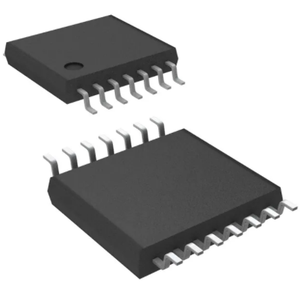


 工商网监
湘ICP备2023018690号
工商网监
湘ICP备2023018690号
