USB Type-C Power Delivery Sink
Controller
Hynetek Semiconductor Co., Ltd.
HUSB238
APPLICATIONS
FEATURES
PD sink devices
USB-C cables
Wireless charger
USB-IF certified
TID: 3666
Standalone USB Power Delivery (PD) sink controller
Legacy charging sink
Apple divider 3 detection
GENERAL DESCRIPTION
The HUSB238 is a highly integrated USB Power
Delivery (PD) controller as sink role for up to 100W
power rating.
BC1.2 SDP, CDP and DCP detection
Dead battery function
SOP’ communication function
3V to 25V operation range
30V voltage rating on VIN and GATE pins
25V voltage rating on CC1 and CC2 pins
I2C access for monitoring and advanced settings
Integrated PMOS driver
VBUS over-voltage protection (OVP) and undervoltage protection (UVP)
Over-temperature protection (OTP) with
programmable thresholds
Low power consumption
The HUSB238 is compatible with PD3.0 and Type-C
V1.4, and it can also support Apple Divider 3, BC1.2
SDP, CDP and DCP while the source is attached.
The HUSB238 can be used in electronic devices that
have legacy barrel connectors or USB micro-B
connectors for power such as IoT (Internet of Things)
devices, wireless charger, drones, smart speakers,
power tools, and other rechargeable devices.
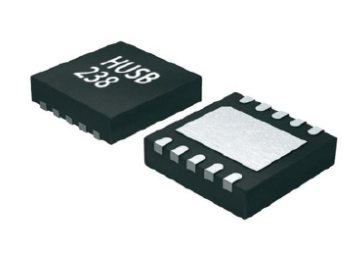
The HUSB238 is available in 3mm x 3mm DFN-10L
and 3.9mm x 4mm SOT33-6L package options.
TYPICAL APPLICATION CIRCUIT
VBUS
POWER
SYSTEM
49.9kΩ
USB-C RECEPTACLE
5.1kΩ
HUSB238
10Ω
VIN
GATE
1μF
CC1
CC2
SCL
CC1
CC2
D+
D+
D-
D-
SOC
SDA
VSET
ISET
GND
22.6kΩ
10kΩ
GND
Figure 1. Typical Application Circuit
©2021-2022 Hynetek Semiconductor Co., Ltd. All rights reserved.
Rev. 2.1
www.hynetek.com
�HUSB238
Data Sheet
TABLE OF CONTENTS
Features ........................................................................................................................................................................... 1
Applications ...................................................................................................................................................................... 1
General Description ......................................................................................................................................................... 1
Typical Application Circuit ................................................................................................................................................ 1
Table of Contents ............................................................................................................................................................. 2
Revision History ............................................................................................................................................................... 2
Pin Configuration and Function Descriptions ................................................................................................................... 3
Recommended Operating Conditions .............................................................................................................................. 4
Specifications ................................................................................................................................................................... 4
Absolute Maximum Ratings ............................................................................................................................................. 6
Thermal Resistance ...................................................................................................................................................... 6
ESD Caution ................................................................................................................................................................. 6
Functional Block Diagram ................................................................................................................................................ 7
Theory of Operation ......................................................................................................................................................... 8
Overview ....................................................................................................................................................................... 8
VIN Pin .......................................................................................................................................................................... 8
GATE Pin ...................................................................................................................................................................... 8
CC1 and CC2 Pins........................................................................................................................................................ 8
VSET Pin....................................................................................................................................................................... 8
ISET Pin ........................................................................................................................................................................ 9
RDO Determination....................................................................................................................................................... 9
Operation With I2C Interface ............................................................................................................................................ 9
Legacy Charger Detection ............................................................................................................................................ 9
Dead Battery Function ................................................................................................................................................ 10
SOP’ Function ............................................................................................................................................................. 10
Over-Voltage Protection .............................................................................................................................................. 10
Under-Voltage Protection ............................................................................................................................................ 10
Over-Temperature Protection...................................................................................................................................... 10
Typical Application Circuits.............................................................................................................................................. 11
Package Outline Dimensions ......................................................................................................................................... 12
Ordering Guide ............................................................................................................................................................... 14
Important Notice ............................................................................................................................................................. 15
REVISION HISTORY
Version
Date
Descriptions
Rev. 1.0
Rev. 2.0
Rev. 2.1
12/2020
01/2021
03/2022
Initial version
Added SOT33-6L package information
Add Recommended Operating Conditions
©2021-2022 Hynetek Semiconductor Co., Ltd. All rights reserved.
Page 2 of 15
�Data Sheet
HUSB238
PIN CONFIGURATION AND FUNCTION DESCRIPTIONS
VIN
6
1
VSET
2
CC1
3
5
CC2
ISET
GND
4
VIN
1
10
GATE
D+
2
9
ISET
11
GND
D-
3
8
VSET
CC1
4
7
SCL
CC2
5
6
SDA
HUSB238
(SOT33-6L)
HUSB238
(DFN-10)
Figure 2. Pin Configuration (Top View)
Table 1. Pin Function Descriptions
Pin No.
Pin Name
DFN-10L
SOT33-6L
Type1
Description
Power supply input. Connect this pin to VBUS of USB Type-C connector
and bias this pin via a 1μF ceramic capacitor.
Positive line of USB 2.0 data line for Apple Divider 3 and BC1.2.
Negative line of USB 2.0 data line for Apple Divider 3 and BC1.2.
Configuration line 1 used to negotiate a voltage/current with the attached
adapter.
Configuration line 2 used to negotiate a voltage/current with the attached
adapter.
I2C communication data signal.
I2C communication clock signal.
Connect a resistor to indicate the maximum voltage needed by the
system from the attached power adapter.
Connect a resistor to indicate the maximum current needed by the
system from the attached power adapter.
Open drain gate driver output. Connect this signal to the gate of an
external PMOS through a series resistor. Leave this pin open if not used.
Ground reference. All signals are referred to this pin.
1
1
VIN
P
2
3
4
−
−
3
D+
DCC1
DIO
DIO
AIO
5
4
CC2
AIO
6
7
8
−
−
2
SDA
SCL
VSET
DIO
DIO
AI
9
6
ISET
AI
10
−
GATE
OD
11
5
GND
P
1 Legend:
A = Analog Pin
P = Power Pin
D = Digital Pin
I = Input Pin
O = Output Pin
OD = Open Drain Pin
©2021-2022 Hynetek Semiconductor Co., Ltd. All rights reserved.
Page 3 of 15
�HUSB238
Data Sheet
RECOMMENDED OPERATING CONDITIONS
Table 2.
Parameter
Rating
VIN Input Voltage Range
Operating Temperature Range (Junction)
Ambient Temperature Range
3.24V to 21V
−40°C to +125°C
-40°C to 85°C
SPECIFICATIONS
VIN = 5V, TA = 25°C, unless otherwise noted.
Table 3.
Parameter
POWER SUPPLY
Supply Voltage
Supply Voltage UVLO Threshold
Supply Current
CC1 AND CC2 PINS
Pull-down Voltage in Dead Battery
Pull-down resistor
Voltage Threshold to Detect a DFP
TX Output Impedance1
Voltage Swing
D+/D- PINS
D- Source Voltage for 0.6V
D+ Source Voltage for 0.6V
Data Detect Voltage
D- Sink Current
D+ Sink Current
D+/D- Comparator Threshold for
2.7V Detection
VSET AND ISET PINS
Source Current
Detect Debounce Time1
Symbol
VIN
VIN_UVLO_RISE
VIN_UVLO_FALL
ISC_OPR
VDBL
VDBH
RD
VTH_DEF
VTH_1P5
VTH_3P0
RTX
Min
Typ
3
Rising edge threshold
Falling edge threshold
VIN = 5V, CC is attached, normal
operation
200μA source current
360μA source current
Max
Unit
25
V
V
V
mA
1.5
2.45
5.6
0.25
0.70
1.31
75
V
V
kΩ
V
V
V
Ω
V
3.1
2.9
3.1
Default current mode
1.5A current mode
3.0A current mode
PD TX mode
0.45
0.85
4.6
0.15
0.61
1.16
33
VDM_SRC
VDP_SRC
VDAT_REF
IDM_SINK
IDP_SINK
VTH_2P7_HI
High threshold for Apple divider 3
0.5
0.5
300
50
50
2.85
0.6
0.6
325
100
100
2.95
0.7
0.7
350
150
150
3.05
V
V
mV
μA
μA
V
VTH_2P7_LO
Low threshold for Apple divider 3
2.25
2.35
2.45
V
IVSET
IISET
tDB_VSET
tDB_ISET
On VSET pin
On ISET pin
For VSET pin
For ISET pin
95
95
100
100
2
2
105
105
μA
μA
ms
ms
5.5
0.4
0.4
V
V
V
V
10
300
mA
Ω
I2C PARAMETERS
Supply Range
Low Level Input Voltage
High Level Input Voltage
Low Level Output Voltage
GATE PIN
Maximum Sink Current1
Pull Low Impedance
1
Test Conditions/Comments
5.1
0.2
0.66
1.23
48
1.125
2.5
Apply for SDA, SCL pins
Apply for SDA, SCL pins
Apply for SDA pin, 2mA load current
1.4
100
Guaranteed by design
©2021-2022 Hynetek Semiconductor Co., Ltd. All rights reserved.
Page 4 of 15
�Data Sheet
Parameter
PROTECTIONS
Over-Voltage Protection Threshold
OVP Debounce Time1
Under-Voltage Protection Threshold
UVP Debounce Time1
Over-Temperature Protection
Threshold1
HUSB238
Symbol
Test Conditions/Comments
Min
Typ
Max
Unit
VVIN_OV
tDB_OV
VVIN_UV
tDB_UV
Refer to VIN
115
120
50
-2
1
150
125
%
μs
V
ms
ᴼC
Refer to VIN
Rising Threshold
Falling Threshold
OTP Debounce Time1
VIN Discharge Resistor
tDB_OT
RDIS
©2021-2022 Hynetek Semiconductor Co., Ltd. All rights reserved.
130
100
500
ᴼC
ms
Ω
Page 5 of 15
�HUSB238
Data Sheet
ABSOLUTE MAXIMUM RATINGS
Table 4.
Parameter
Rating
VIN, GATE
CC1, CC2
D+, D−
VSET, ISET, SDA, SCL
Operating Temperature Range (Junction)
Soldering Conditions
Electrostatic Discharge (ESD)
Human Body Mode (HBM)
−0.3V to +30V
−0.3V to +25V
−0.3V to +12V
−0.3V to +6V
−40°C to +125°C
JEDEC J-STD-020
±6000V
Stresses at or above those listed under Absolute Maximum Ratings may cause permanent damage to the product.
This is a stress rating only; functional operation of the product at these or any other conditions above those indicated
in the operational section of this specification is not implied. Operation beyond the maximum operating conditions for
extended periods may affect product reliability.
THERMAL RESISTANCE
Thermal performance is directly linked to printed circuit board (PCB) design and operating environment. Close
attention to PCB thermal design is required.
θJA is the natural convection junction to ambient thermal resistance measured in a one cubic foot sealed enclosure.
θJC is the junction to case thermal resistance.
Table 5. Thermal Resistance
Package Type
DFN-10L
SOT33-6L
θJA
θJC
Unit
75
89
54
27
°C/W
°C/W
ESD CAUTION
Electrostatic Discharge Sensitive Device.
Charged devices and circuit boards can discharge without detection. Although this product features patented
or proprietary protection circuitry, damage may occur on devices subjected to high energy ESD. Therefore,
proper ESD precautions should be taken to avoid performance degradation or loss of functionality.
©2021-2022 Hynetek Semiconductor Co., Ltd. All rights reserved.
Page 6 of 15
�Data Sheet
HUSB238
FUNCTIONAL BLOCK DIAGRAM
GATE
DRIVER
VIN
RDIS
POR
CIRCUIT
VOLTAGE
REGULATOR
D+
D-
CC1
CC2
OV & UV
PROTECTION
IVSET
VREG
GND
VSET
ISET
APPLE MODE
BC1.2
DETECTION
USB PD
PHYSICAL
LAYER
GATE
PORT
CONTROLLER
USB PD
PROTOCAL
LAYER
IISET
SDA
OTP
I2C ENGINE
SCL
Figure 3. HUSB238 Functional Block Diagram
©2021-2022 Hynetek Semiconductor Co., Ltd. All rights reserved.
Page 7 of 15
�HUSB238
Data Sheet
THEORY OF OPERATION
OVERVIEW
The HUSB238 is a highly integrated USB Power Delivery (PD) controller as sink role. It’s compatible with PD3.0 and
Type-C V1.4. It can also support Apple Divider 3, BC1.2 SDP, DCP and CDP while source is attached. When
HUSB238 is connected to power source, it applies Rd to both CC lines, trying to establish USB Type-C connection.
After the USB Type-C connection is established, it monitors the CC lines to get source capabilities pack from USB PD
source. If there is valid source capabilities pack before time out, the HUSB238 policy engine requests a power supply
with voltage no greater than the programmed request voltage. If there is no valid source capabilities pack after time
out, the HUSB238 switches to Apple divider 3 or BC1.2 mode trying to determine corresponding charging protocol.
VIN PIN
VIN pin is the power supply input of the HUSB238, which is derived from the output of the PD source. Connect a 1µF
decoupling MLCC between VIN pin and GND pin as closer as possible.
The VIN pin is also connected to an internal MOSFET and 500Ohm discharging resistor, which is used as a bleeder to
help discharge the output capacitor to vSafe5V upon the hard reset, over-voltage fault, over-temperature fault or
detachment of a connected device.
GATE PIN
The GATE pin is open–drain output which allows to drive an external PMOS load switch directly. The GATE pin can be
programmed to turn on after POR or after the explicit contract. The default option is to turn on after POR. Please
contact local Hynetek sales for a device with options other than the default option.
CC1 AND CC2 PINS
CC1 and CC2 are the Configuration Channel pins used for connection and attachment detection, plug orientation
determination and system configuration management across USB Type-C cable. CC1 and CC2 pins can support as
high as 25V voltage, which is used for protection when CC1 or CC2 is shorted to VBUS pin on the connector.
Through the Type-C detection, one of the CC pin is connected to the internal BMC block to achieve PD
communication.
VSET PIN
A fixed 100μA current source is applied on VSET pin. Connect a resister between VSET and GND to indicate the
VSET_VOLTAGE value as shown in Table 6.
Table 6. VSET_VOLTAGE Setting
RVSET (kΩ)
VSET_VOLTAGE (V)
0
6.04
10
14
17.8
Open
5
9
12
15
18
20
The RDO voltage of the HUSB238 is determined by the lower value between VSET_VOLTAGE and
SNK_PDO2_VOLTAGE. SNK_PDO2_VOLTAGE is programmable by internal fuse options and the default value is
20V. The requested voltage value can be changed dynamically with the resistance value change.
©2021-2022 Hynetek Semiconductor Co., Ltd. All rights reserved.
Page 8 of 15
�Data Sheet
HUSB238
ISET PIN
A fixed 100μA current source is applied on ISET pin. Connect a resister between ISET and GND to indicate the
ISET_CURRENT value as shown in Table 7.
Table 7. ISET_CURRENT Setting
RISET (kΩ)
ISET_CURERNT (A)
0
4.53
7.5
10.5
13.7
16.5
19.6
22.6
Open
1.25
1.5
1.75
2
2.25
2.5
2.75
3
3.25
The RDO current of the HUSB238 is determined by the lower value between ISET_CURRENT and
SNK_PDO2_CURRENT. SNK_PDO2_CURRENT is programmable by internal fuse options and the default value is
3.25A. The requested current value can be changed dynamically with the resistance value change.
RDO DETERMINATION
There are two ways to determine the RDO that the HUSB238 requests from the PD source. Set by the VSET and
ISET pins or set by the internal factory programmed fuse options. The HUSB238 compares the two values and uses
the lower value as its RDO.
For example, if the VSET and ISET is configured as 9V / 3A. The internal factory fuse option is 12V / 2A. Then the
RDO that HUSB238 requests from the PD source is 9V / 2A.
After the RDO is determined, the HUSB238 loops through the PD source PDOs from highest voltage first to find the
first PDO that satisfies the following conditions:
1. SOURCE_PDO_VOLTAGE ≤ RDO_VOLTAGE
2. SOURCE_PDO_CURRENT ≥ RDO_CURRENT
If both the conditions above are satisfied, then HUSB238 sends a request for this source PDO with operating current
set to the RDO current value.
If either one of the condition is not satisfied, the HUSB238 continues to compare with the second highest voltage
source PDO or requests 5V source PDO directly, depending on the internal fuse options. The default fuse option is to
continue to compare with the second highest voltage source PDO. Please contact local Hynetek sales for a device
with options other than the default option.
OPERATION WITH I2C INTERFACE
The HUSB238 is I2C communication capable with system MCU or processor through SDA and SCL pins. The
HUSB238 works as I2C slave role and the I2C address is 0x08.
After POR (Power On Reset), the HUSB238 receives the source capability information from the PD source adapter
and the HUSB238 saves the source capability information in registers. The system MCU can visit the HUSB238
registers through the I2C bus and select a proper PDO to request from external PD source.
The I2C has the highest priority. If using I2C to select a source PDO, it over writes the internal RDO which is created
by VSET, ISET pins and internal factory fuse option, and the HUSB238 requests the I2C selected source PDO once
the I2C commands are written.
LEGACY CHARGER DETECTION
After the power on reset, if the HUSB238 does not establish PD contract with source adapter, the HUSB238 will waits
for 1.5 seconds and then switches to Apple Divider 3 and BC1.2 detections sequentially. For BC1.2 detection, the
HUSB238 detects SDP (Standard Data Port), CDP (Charging Data Port) and DCP (Dedicated Charging Port)
sequentially.
©2021-2022 Hynetek Semiconductor Co., Ltd. All rights reserved.
Page 9 of 15
�HUSB238
Data Sheet
DEAD BATTERY FUNCTION
The HUSB238 works as PD sink role which requires RD resistor to be presented on the CC pins even in the unpowered state for successful Type-C detection by source adapter.
The dead battery function in the HUSB238 supports default USB, 1.5A and 3.0A source broadcast RP current.
SOP’ FUNCTION
For the USB-C to legacy PC plug applications where high current and high voltage are required, the system needs
current more than 3A in most of the cases. If the SOP’ function is enabled, the HUSB238 is capable to reply SOP’
command, such as Discover Identity, sent by the PD source adapter.
The SOP’ function emulates the E-Marker function in the cable so that the system is capable of obtaining more than
3A charging current from PD source adapter.
OVER-VOLTAGE PROTECTION
The HUSB238 senses the voltage on VIN pin for overvoltage protection. The over-voltage threshold is 1.2 times of
max requested voltage. The OV debounce time is 50μs.
When OV happens, the HUSB238 turns off the external PMOS and enters into discharge mode where the internal
discharge circuit on VIN pin is turned on. The internal 5.1k Rd resistor is also disconnected during discharge mode.
After the discharge timeout, the HUSB238 enters into unattached mode and waits for re-connection with PD source
adapter.
UNDER-VOLTAGE PROTECTION
The HUSB238 senses the voltage on VIN pin for optional under-voltage protection. The under-voltage threshold is the
requested voltage minus 2V. For example, if the requested PDO voltage is 12V, then the UV threshold is 10V. The UV
debounce time is 1ms.
When UV happens, the HUSB238 turns off the external PMOS and enters into discharge mode where the internal
discharge circuit on VIN pin is turned on. The internal 5.1k Rd resistor is also disconnected during discharge mode.
After the discharge timeout, the HUSB238 enters into unattached mode and waits for re-connection with PD source
adapter.
The UVP function of the HUSB238 can be enabled or disabled by internal fuse options. The UVP function is disabled
for default option. Please contact local Hynetek sales for a device with options other than the default option.
OVER-TEMPERATURE PROTECTION
The HUSB238 integrates over-temperature protection function. It monitors the internal junction temperature. When the
junction temperature reaches the over temperature rising threshold, the HUSB238 requests 5V source PDO directly,
regardless of the previous established PDO, to reduce the total system power. When the junction temperature falls
below the over temperature falling threshold, the HUSB238 re-negotiates the previous PDO and tries to recover the
normal charging operation.
The over temperature thresholds are programmable by internal factory fuses. Please contact local Hynetek sales for a
device with options other than the default option.
©2021-2022 Hynetek Semiconductor Co., Ltd. All rights reserved.
Page 10 of 15
�Data Sheet
HUSB238
TYPICAL APPLICATION CIRCUITS
BATTERY
VBUS
DC-DC Reg
Or Charger
49.9kΩ
+
USB-C RECEPTACLE
5.1kΩ
VIN
GATE
HUSB238
DFN-10
1μF
CC1
CC1
CC2
CC2
D+
D+
D-
D-
SCL
SOC
SDA
VSET
ISET
GND
GND
Figure 4. USB-C Device Application
VBUS
VIN
HUSB238
SOT33-6
1μF
CC1
CC1
CC2
CC2
VSET
ISET
GND
LEGACY CHARGING
CONNECTOR
USB-C CONNECTOR
VIN
1kΩ
GND
GND
Figure 5. USB-C Cable Application
©2021-2022 Hynetek Semiconductor Co., Ltd. All rights reserved.
Page 11 of 15
�HUSB238
Data Sheet
PACKAGE OUTLINE DIMENSIONS
Figure 6. DFN-10L Package, 3 mm × 3 mm
©2021-2022 Hynetek Semiconductor Co., Ltd. All rights reserved.
Page 12 of 15
�Data Sheet
HUSB238
Figure 7. SOT33-6L Package, 3.9 mm x 4.0 mm
©2021-2022 Hynetek Semiconductor Co., Ltd. All rights reserved.
Page 13 of 15
�HUSB238
Data Sheet
ORDERING GUIDE
Model
Package
SOP’
OTP Threshold
RDO Mismatch Action
Package Option
HUSB238_001DD
HUSB238_002DD
HUSB238_002SH
HUSB238_003DD
HUSB238_003SH
HUSB238_004DD
DFN-10L
DFN-10L
SOT33-6L
DFN-10L
SOT33-6L
DFN-10L
YES
NO
NO
YES
YES
NO
90°C / 75°C
150°C / 130°C
150°C / 130°C
90°C / 75°C
90°C / 75°C
150°C / 130°C
Request 5V
Next PDO
Next PDO
Next PDO
Next PDO
Request 5V
Tape & Reel, 4k
Tape & Reel, 4k
Tape & Reel, 7.5k
Tape & Reel, 4k
Tape & Reel, 7.5k
Tape & Reel, 4k
©2021-2022 Hynetek Semiconductor Co., Ltd. All rights reserved.
Page 14 of 15
�Data Sheet
HUSB238
IMPORTANT NOTICE
Hynetek Semiconductor Co., Ltd. and its subsidiaries (Hynetek) reserve the right to make corrections, enhancements,
improvements and other changes to its semiconductor products and services per JESD46, latest issue, and to discontinue any
product or service per JESD48, latest issue. Buyers should obtain the latest relevant information before placing orders and should
verify that such information is current and complete. All semiconductor products (also referred to herein as “components”) are sold
subject to Hynetek’s terms and conditions of sale supplied at the time of order acknowledgment.
Hynetek warrants performance of its components to the specifications applicable at the time of sale, in accordance with the
warranty in Hynetek’s terms and conditions of sale of semiconductor products. Testing and other quality control techniques are
used to the extent Hynetek deems necessary to support this warranty. Except where mandated by applicable law, testing of all
parameters of each component is not necessarily performed.
Hynetek assumes no liability for applications assistance or the design of Buyers’ products. Buyers are responsible for their
products and applications using Hynetek components. To minimize the risks associated with Buyers’ products and applications,
Buyers should provide adequate design and operating safeguards.
Hynetek does not warrant or represent that any license, either express or implied, is granted under any patent right, copyright,
mask work right, or other intellectual property right relating to any combination, machine, or process in which Hynetek components
or services are used. Information published by Hynetek regarding third-party products or services does not constitute a license to
use such products or services or a warranty or endorsement thereof. Use of such information may require a license from a third
party under the patents or other intellectual property of the third party, or a license from Hynetek under the patents or other
intellectual property of Hynetek.
Reproduction of significant portions of Hynetek information in Hynetek data books or data sheets is permissible only if reproduction
is without alteration and is accompanied by all associated warranties, conditions, limitations, and notices. Hynetek is not
responsible or liable for such altered documentation. Information of third parties may be subject to additional restrictions.
Resale of Hynetek components or services with statements different from or beyond the parameters stated by Hynetek for that
component or service voids all express and any implied warranties for the associated Hynetek component or service and is an
unfair and deceptive business practice.
Hynetek is not responsible or liable for any such statements.
Buyer acknowledges and agrees that it is solely responsible for compliance with all legal, regulatory and safety-related
requirements concerning its products, and any use of Hynetek components in its applications, notwithstanding any applicationsrelated information or support that may be provided by Hynetek. Buyer represents and agrees that it has all the necessary
expertise to create and implement safeguards which anticipate dangerous consequences of failures, monitor failures and their
consequences, lessen the likelihood of failures that might cause harm and take appropriate remedial actions. Buyer will fully
indemnify Hynetek and its representatives against any damages arising out of the use of any Hynetek components in safety-critical
applications.
In some cases, Hynetek components may be promoted specifically to facilitate safety-related applications. With such components,
Hynetek’s goal is to help enable customers to design and create their own end-product solutions that meet applicable functional
safety standards and requirements. Nonetheless, such components are subject to these terms.
No Hynetek components are authorized for use in FDA Class III (or similar life-critical medical equipment) unless authorized
officers of the parties have executed a special agreement specifically governing such use.
Only those Hynetek components which Hynetek has specifically designated as military grade or “enhanced plastic” are designed
and intended for use in military/aerospace applications or environments. Buyer acknowledges and agrees that any military or
aerospace use of Hynetek components which have not been so designated is solely at the Buyer's risk, and that Buyer is solely
responsible for compliance with all legal and regulatory requirements in connection with such use.
Hynetek has specifically designated certain components as meeting ISO/TS16949 requirements, mainly for automotive use. In any
case of use of non-designated products, Hynetek will not be responsible for any failure to meet ISO/TS16949.
Please refer to below URL for other products and solutions of Hynetek Semiconductor Co., Ltd.
©2021 Hynetek Semiconductor Co., Ltd. All rights reserved.
Trademarks and registered trademarks are the property of their respective owners.
www.hynetek.com
©2021-2022 Hynetek Semiconductor Co., Ltd. All rights reserved.
Page 15 of 15
�