AnalogTek
AT8563
——A low power RTC chip with I2C
Document No.:
AT8563DS001V1.2E
Issued Date:
2009.2.23
February 25, 2009
�CONTENTS
1
Chip Overview ............................................................................................................................ 1
2
Functional Description ................................................................................................................ 2
2.1
Summary .......................................................................................................................... 2
2.2
Alarm function modes ...................................................................................................... 4
2.3
Timer ................................................................................................................................ 4
2.4 CLKOUT output .............................................................................................................. 4
3
2.5
Reset ................................................................................................................................. 4
2.6
Voltage-low detector ........................................................................................................ 4
2.7
Register organization ....................................................................................................... 5
2.7.1
Control/Status 1 register ........................................................................................ 6
2.7.2
Control/Status 2 register ........................................................................................ 6
2.7.3
Seconds, Minutes and Hours registers .................................................................. 7
2.7.4
Days, Weekdays, Months/Century and Years registers ........................................ 7
2.7.5
Alarm registers ...................................................................................................... 9
2.7.6
CLKOUT frequency register ............................................................................... 10
2.7.7
Countdown timer registers .................................................................................. 10
2.8
EXT_CLK test mode...................................................................................................... 11
2.9
Power-On Reset override mode ..................................................................................... 12
Serial interface .......................................................................................................................... 12
3.1
I2C Specification ............................................................................................................ 12
3.2
I2C of AT8563 ................................................................................................................ 14
4
Parameters ................................................................................................................................. 15
5
Application Reference............................................................................................................... 19
5.1
6
Crystal frequency adjustment ......................................................................................... 19
Package outline ......................................................................................................................... 20
6.1
DIP-8 .............................................................................................................................. 20
6.2
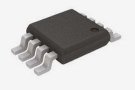
SO8 ................................................................................................................................ 21
6.3
TSSOP8 .......................................................................................................................... 21
6.4
MSOP8 ........................................................................................................................... 22
�AT8563DS001V1.2E
1
Chip Overview
AT8563 is a CMOS real-time clock/calendar chip optimized for low power consumption.
The timing counter consists of century, year, month, day, date, hour, minute and second bits.
External MPU can read or set the time as well as timer or alarmer when it is necessary. As
exchanging data by the advance serial bus I2C, lines number on PCB can be reduced
dramatically, which is very suitable in a complicated system.
The chip has the following features:
An external 32.768 kHz crystal is needed to generated time base
Wide operating supply voltage range: 1.0 to 5.5 V
Low back-up current; typical 0.25 µA at VDD = 3.0 V and Tamb = 25 °C
400 kHz two-wire I2C-bus interface (at VDD = 1.8 to 5.5 V)
Programmable clock output for peripheral devices: 32.768 kHz, 1024 Hz 32 Hz
and 1 Hz
Alarm and timer functions
Voltage-low detector
Integrated oscillator capacitor
Internal power-on reset
I2C-bus slave address: read A3H; write A2H
Typical Applications:
Mobile telephones
Portable instruments
OA equipments such as Fax machines
Battery powered products
Table 1 shows our ordering information for AT8563.
Table1
Ordering information
Type number
Package
Name
Name
Description
Version
AT8563P
DIP8
plastic dual in-line package; 8 leads (300 mil)
SOT97-1
AT8563T
SO8
plastic small outline package; 8 leads; body width 3.9 mm
SOT96-1
AT8563TS
SSO8
plastic small outline package; 8 leads; body width 3.0 mm
SOT505-1
AT8563S
MSOP8
plastic small outline package; 8 leads; body width 3.0 mm
•
1
•
�AT8563DS001V1.2E
Table 2 Quick reference data
Symol
Parameter
Conditions
Min
Max
Unit
1.0
5.5
V
1.8
5.5
V
fSCL = 200 kHz
800
µA
fSCL = 100 kHz
200
µA
550
µA
I2C-bus inactive; Tamb = 25 °
VDD
supply voltage operating mode
supply crrent; timer and CLKOUT
disabled
IDD
2
I C-bus active; fSCL = 400 kHz;
Tamb = −30 to +85°C
fSCL = 0 Hz; Tamb= 25 °C
VDD = 5 V
450
µA
Tamb
operating ambient temperature
VDD = 2 V
-
−30
+85
°C
Tstg
storage temperature
-
−65
+150
°C
2
Functional Description
2.1
Summary
The device’s structure is shown in Fig 1.
Fig 1 Block diagram
AT8563’s pin layout and its protection network are shown in Fig 2 and Fig 3.
•
2
•
�AT8563DS001V1.2E
Fig 2 Pin Layout
Fig 3 Device diode protection diagram
Table 3 gives the pins’ description.
Table 3: Pin description
Symbol
Pin
Description
OSCI
1
oscillator input
OSCO
2
oscillator output
INT
3
interrupt output (open-drain; active LOW)
VSS
4
ground
SDA
5
serial Data I/O (open-drain)
SCL
6
serial Clock in
CLKOUT
7
clock output (open-drain)
VDD
8
positive power supply
AT8563 contains sixteen 8-bit registers with an auto-increasing address register, an
on-chip 32.768 kHz oscillator with an integrated capacitor, a frequency divider which provides
source clock for the Real-Time Clock (RTC), a programmable clock output, a timer, an alarm, a
voltage-low detector and a I2C-bus interface.
The 16 registers are mapped into a memory block, which is addressable, but not all bits
are implemented. The first two registers (memory address 00H and 01H) are used as control
and/or status registers. The memory addresses 02H through 08H are used as counters for the
clock function (seconds up to year counters). Address locations 09H through 0CH contain
alarm registers which define the conditions for an alarm. Address 0DH controls the frequency
of CLKOUT output. 0EH and 0FH are timer control, timer counter register, respectively.
The Seconds, Minutes, Hours, Days, Months, Years as well as the Minute alarm, Hour
alarm and Day alarm registers are all coded in BCD format. The Weekdays and Weekday
alarm register are not coded in BCD format.
When one of the RTC registers is read the contents of all counters are frozen. Therefore,
faulty reading of the clock/calendar during a carry condition is prevented.
•
3
•
�AT8563DS001V1.2E
2.2
Alarm function modes
———
By clearing the MSB (bit AE = Alarm Enable) of one or more of the alarm registers, the
corresponding alarm condition(s) will be active. In this way an alarm can be generated from
once per minute up to once per week. The alarm condition sets the alarm flag, AF (bit 3 of
Control/Status 2 register). The asserted AF can be used to generate an interrupt (INT). Bit AF
can only be cleared by software.
2.3
Timer
The 8-bit countdown timer (address 0FH) is controlled by the Timer Control register
(address 0EH; see Table 25). The Timer Control register selects one of 4 source clock
frequencies for the timer (4096, 64, 1, or 1⁄60 Hz), and enables/disables the timer. The timer
counts down from a software-loaded 8-bit binary value. At the end of every countdown, the
timer sets the timer flag TF (see Table 7). The timer flag TF can only be cleared by software.
The asserted timer flag TF can be used to generate aninterrupt (INT). The interrupt may be
generated as a pulsed signal every countdownperiod or as a permanently active signal which
follows the condition of TF. TI/TP (seeTable 7) is used to control this mode selection. When
reading the timer, current countdown value is returned.
2.4
CLKOUT output
A programmable square wave is available at the CLKOUT pin. Operation is controlled by
the CLKOUT frequency register (address 0DH; see Table 23). Frequencies of 32.768 kHz
(default), 1024, 32 and 1 Hz can be generated for use as a system clock, microcontroller clock,
input to a charge pump, or for calibration of the oscillator. CLKOUT is an open-drain output
and enabled at power-on. If disabled it becomes high-impedance.
2.5
Reset
AT8563 includes an internal reset circuit which is active whenever the oscillator is
stopped. In the reset state the I2C-bus logic is initialized and all registers, including the address
———
pointer, are cleared with the exception of bits FE, VL, TD1, TD0, TESTC and AE which are set
to logic 1.
2.6
Voltage-low detector
AT8563 has an on-chip voltage-low detector. When VDD drops below Vlow the VL bit
(Voltage Low, bit 7 in the Seconds register) is set to indicate that reliable clock/calendar
information is no longer guaranteed. The VL flag can only be cleared by software.
The VL bit is intended to detect the situation when VDD is decreasing slowly for example
under battery operation. Should VDD reach Vlow before power is re-asserted then the VL bit will
be set. This will indicate that the time may have been corrupted.
•
4
•
�AT8563DS001V1.2E
Fig 4 Voltage-low detection
2.7
Register organization
Table 4
Registers overview
Address
Register name
b7
b6
b5
b4
b3
b2
b1
b0
00H
01H
0DH
0EH
Control/Status 1
Control/Status 2
CLKOUT frequency
Timer control
TEST1
0
FE
TE
0
0
-
STOP
0
-
0
TI/TP
-
TESTC
AF
-
0
TF
-
0
AIE
FD1
TD1
0
TIE
FD0
TD0
0FH
Timer countdownvalue
Note: Bit positions labeled as ‘− ’are not implemented; those labeled with ‘0’ should always be written with
logic 0.
Table 5
BCD formatted registers overview
Address
Register name
b7
b6
b5
b4
02H
Seconds
VL
ten seconds(0-5)
seconds(0-9)
03H
minutes
-
ten minutes(0-5)
minutes(0-9)
04H
hours
-
-
ten hours(0-2)
hours(0-9)
05H
days
-
-
ten days(0-3)
days(0-9)
06H
weekday
-
-
-
07H
months/century
C
-
-
08H
years
-
b3
-
ten month
09H
minute alarm
0AH
hour alarm
———
0BH
day alarm
———
0CH
weekday alarm
———
AE
AE
AE
AE
b1
weekdays(0-6)
years(0-9)
ten minutes(0-5)
minutes(0-9)
-
ten hours(0-2)
hours(0-9)
-
ten days(0-3)
days(0-9)
-
-
Note: Bit positions labelled as ‘− ’are not implemented.
•
5
•
b0
month(0-9)
(0-1)
ten years(0-9)
———
b2
-
-
weekdays(0-6)
�AT8563DS001V1.2E
2.7.1 Control/Status 1 register
Table 6
00H
Symbol
b7
TEST1
b5
STOP
b3
TESTC
b6, b4,
b2..0
-
Control/Status 1 register bits description
Description
TEST1 = 0; normal mode.
TEST1 = 1; EXT_CLK test mode; see Section 8.7.
STOP = 0; RTC source clock runs.
STOP = 1; all RTC divider chain flip-flops are asynchronously set to logic 0; the
RTC clock is stopped (CLKOUT at 32.768 kHz is still available).
TESTC = 0; power-on reset override facility is disabled (set to logic 0 for normal
operation).
TESTC = 1; power-on reset override is enabled.
By default set to logic 0.
2.7.2 Control/Status 2 register
Table 7
01H
Symbol
b7..5
0
b4
TI/TP
b3
AF
b2
TF
b1
AIE
b0
TIE
Description of Control/Status 2 register bits description
Description
By default set to logic 0
TI/TP = 0: INT is active when TF is active (subject to the status of TIE).
TI/TP = 1: INT pulses active according to Table 8 (subject to the status of TIE). Note
that if AF and AIE are active then INT will be permanently active.
When an alarm occurs, AF is set to logic 1. Similarly, at the end of a timer
countdown, TF is set to logic 1. These bits maintain their value until overwritten by
software. If both timer and alarm interrupts are required in the application, the source
of the interrupt can be determined by reading these bits. To prevent one flag being
overwritten while clearing another, a logic AND is performed during a write access.
See Table 9 for the value descriptions of bits AF and TF.
Bits AIE and TIE activate or deactivate the generation of an interrupt when AF or TF
is asserted, respectively. The interrupt is the logical OR of these two conditions
when both AIE and TIE are set.
AIE = 0: alarm interrupt disabled; AIE = 1: alarm interrupt enabled.
TIE = 0: timer interrupt disabled; TIE = 1: timer interrupt enabled.
———
Table 8
INT operation (bit TI/TP = 1)
———
INT period(s)
Source clock (Hz)
n=1
n>1
4096
1/8192
1/4096
64
1/128
1/64
1
1/64
1/64
1/60
1/64
1/64
Note:
———
[1] TF and INT become active simultaneously.
[2] n = loaded countdown timer value. Timer stopped when n = 0.
•
6
•
�AT8563DS001V1.2E
Table 9
Value descriptions for bits AF and TF
Bit: AF
Bit: TF
R/W
Value
Description
Value
Description
0
alarm flag inactive
0
timer flag inactive
1
alarm flag active
1
timer flag active
0
alarm flag is cleared
0
timer flag is cleared
1
alarm flag remains unchanged
1
timer flag remains unchanged
Read
Write
2.7.3
Seconds, Minutes and Hours registers
Table 10: Seconds/VL register bits description
02H
Symbol
Description
b7
VL
b6..0
VL = 0: reliable clock/calendar information is guaranteed;
VL = 1: reliable clock/calendar information is no longer guaranteed.
These bits represent the current seconds value coded in BCD format; value
= 00 to 59.
Example: = 101 1001, represents the value 59 s.
Table 11 Minutes register bits description
03H
Symbol
b7
-
b6..0
Description
not implemented
These bits represent the current minutes value coded in BCD
format; value = 00 to 59.
Table 12
04H
Symbol
b7..6
-
b5..0
2.7.4
Hours register bits description
Description
not implemented
These bits represent the current hours value coded in BCD format; value = 00
to 23.
Days, Weekdays, Months/Century and Years registers
Table 13
05H
Symbol
b7..6
-
Days register bits description
Description
not implemented
•
7
•
�AT8563DS001V1.2E
b5..0
These bits represent the current day value coded in BCD format; value = 01 to
31.
AT8563 compensates for leap years by adding a 29th day to February if the year
counter contains a value which is exactly divisible by 4, including the year ‘00’.
Table 14
06H
Symbol
b7..3
b2..0
Weekdays register bits description
Description
-
not implemented
These bits represent the current weekday value 0 to 6, whose
meaning is customized by users. However, we recommend a way
to specify the weekday number, see Table 15.
These bits may be re-assigned by the user.
Table 15
Suggested Weekday assignments
Day
Bit 2
Bit 1
Bit 0
Sunday
Monday
Tuesday
Wednesday
Thursday
Friday
Saturday
0
0
0
0
1
1
1
0
0
1
1
0
0
1
0
1
0
1
0
1
0
Table 16 Months/Century register bits description
07H
Symbol
Description
b7
C
Century bit. C = 0; indicates the century is 20xx.
C = 1; indicates the century is 19xx. ‘xx’ indicates the value held in the
Years register; see Table 18.
This bit is toggled when the Years register overflows from 99 to 00.
These bits may be re-assigned by the user
b6..5
-
not implemented
b4..0
These bits represents the current month value coded in BCD format;
value = 01 to 12; see Table 17.
Table 17
Month assignments
Month
Bit 4
Bit 3
Bit 2
Bit 1
Bit 0
January
0
0
0
0
1
February
0
0
0
1
0
March
0
0
0
1
1
April
0
0
1
0
0
May
0
0
1
0
1
June
0
0
1
1
0
•
8
•
�AT8563DS001V1.2E
July
0
0
1
1
1
August
0
1
0
0
0
September
0
1
0
0
1
October
1
0
0
0
0
November
1
0
0
0
1
December
1
0
0
1
0
Table 18
2.7.5
Years register bits description
08H
Symbol
Description
b7..0
This register represents the current year value coded in BCD format; value
= 00 to 99.
Alarm registers
When one or more of the alarm registers are loaded with a valid minute, hour, day or
———
weekday and its corresponding AE (Alarm Enable) bit is a logic 0, then that information will be
compared with the current minute, hour, day and weekday. When all enabled comparisons first
match, the bit AF (Alarm Flag) is set.
AF will remain set until cleared by software. Once AF has been cleared it will only be set
again when the time increments to match the alarm condition once more. Alarm registers
———
which have their AE bit set at logic 1 will be ignored.
Table 19 Minute alarm register bits description
09H
b7
b6..0
Symbol
Description
———
———
These bits represents the minute alarm information coded in BCD
format; value = 00 to 59.
Table 20
0AH
7
6 to
0
———
A E = 0; minute alarm is enabled. A E = 1; minute alarm is disabled.
AE
Hour alarm register bits description
Symbol
Description
———
———
AE
———
A E = 0; hour alarm is enabled. A E = 1; hour alarm is disabled.
These bits represents the hour alarm information coded in BCD
format; value = 00 to 23.
Table 21: Day alarm register bits description
0BH
b7
Symbol
———
AE
Description
———
———
A E = 0; day alarm is enabled. A E = 1; day alarm is disabled.
•
9
•
�AT8563DS001V1.2E
b6..0
These bits represents the day alarm information coded in BCD
format; value = 01 to 31.
Table 22
0CH
Weekday alarm register bits description
Symbol
Description
———
b6..0
2.7.6
A E = 0; weekday alarm is enabled.
———
b7
AE
———
A E = 1; weekday alarm is disabled.
These bits represents the weekday alarm information
value 0 to 6.
CLKOUT frequency register
Table 23
CLKOUT frequency register bits description
0DH
Symbol
Description
b7
FE
FE = 0; the CLKOUT output is inhibited and the CLKOUT output is set to
high-impedance. FE = 1; the CLKOUT output is activated.
b6..2
-
b1
FD1
b0
FD0
not implemented
These bits control the frequency output (fCLKOUT) on the CLKOUT pin; see
Table 24.
Table 24
CLKOUT frequency selection
FD1
FD0
fCLKOUT
0
0
32.768 kHz
0
1
1 024 Hz
1
0
32 Hz
1
1
1 Hz
2.7.7 Countdown timer registers
The Timer register is an 8-bit binary countdown timer. It is enabled and disabled via the
Timer control register bit TE. The source clock for the timer is also selected by the Timer
control register. Other timer properties, e.g. interrupt generation, are controlled via the
Control/status 2 register. For accurate read back of the countdown value, the I2C-bus clock
SCL must be operating at a frequency of at least twice the selected timer clock.
Table 25
0EH
Symbol
b7
TE
b6~b2
-
Timer control register bits description
Description
TE = 0; timer is disabled. TE = 1; timer is enabled.
not implemented
•
10
•
�AT8563DS001V1.2E
0EH
Symbol
Description
b1
TD1
b0
TD0
Timer source clock frequency selection bits. These bits
determine the source clock for the countdown timer, see
Table 26. When not in use, TD1 and TD0 should be set to
‘11’ (1⁄60 Hz) for power saving.
Table 26
Table 27
2.8
Timer source clock frequency selection
TD[1:0]
Timer source clock
frequency(Hz)
00
4096
01
64
10
1
11
1/60
Timer countdown value register bits description
0FH
Symbol
Description
b7~b0
countdown value n, the counter’s period is “”n/fCLK”
EXT_CLK test mode
A test mode is available which allows for on-board testing. In this mode it is possible to set
up test conditions and control the operation of the RTC.
The test mode is entered by setting bit TEST1 in the Control/Status1 register. The
CLKOUT pin then becomes an input. The test mode replaces the internal 64 Hz signal with the
signal that is applied to the CLKOUT pin. Every 64 positive edges applied to CLKOUT will then
generate an increment of one second.
The signal applied to the CLKOUT pin should have a minimum pulse width of 300 ns and
a minimum period of 1000 ns. The internal 64 Hz clock, now sourced from CLKOUT, is divided
down to 1 Hz by a 26 divide chain called a pre-scaler. The pre-scaler can be set into a known
state by using the STOP bit. When the STOP bit is set, the pre-scaler is reset to 0. STOP must
be cleared before the pre-scaler can operate again. From a STOP condition, the first 1 s
increment will take place after 32 positive edges on CLKOUT. Thereafter, every 64 positive
edges will cause a 1 s increment.
Remark: Entry into EXT_CLK test mode is not synchronized to the internal 64 Hz clock.
When entering the test mode, no assumption as to the state of the pre-scaler can be made.
You can operate in the following steps:
1. Enter the EXT_CLK test mode; set bit 7 of Control/Status 1 register (TEST = 1)
2. Set bit 5 of Control/Status 1 register (STOP = 1)
3. Clear bit 5 of Control/Status 1 register (STOP = 0)
4. Set time registers (Seconds, Minutes, Hours, Days, Weekdays, Months/Century and
Years) to desired value
•
11 •
�AT8563DS001V1.2E
5. Apply 32 clock pulses to CLKOUT
6. Read time registers to see the first change
7. Apply 64 clock pulses to CLKOUT
8. Read time registers to see the second change.
Repeat steps 7 and 8 for additional increments if necessary.
2.9
Power-On Reset override mode
The POR duration is directly related to the crystal oscillator start-up time. Due to the long
start-up times experienced by these types of circuits, a mechanism has been built in to disable
the POR and hence speed up on-board test of the device. The setting of this mode requires
that the I2C-bus pins, SDA and SCL, be toggled in a specific order as shown in Fig 5. All timing
values are required minimum.
Once the override mode has been entered, the chip immediately stops being reset and
normal operation starts i.e. entry into the EXT_CLK test mode via I2C-bus access. The
override mode is cleared by writing a logic 0 to bit TESTC. Re-entry into the override mode is
only possible after TESTC is set to logic 1. Setting TESTC to logic 0 during normal operation
has no effect except to prevent entry into the POR override mode.
Fig 5 POR override sequence.
3
Serial interface
The serial interface of AT8563 is the I2C -bus, which requires minimum connections
between MPU and it peripherals ——.a serial Data I/O line and a serial CLK line driven by
MPU.
3.1
I2C Specification
The I2C -bus is for bidirectional, two-line communication between different ICs or modules.
The two lines are a serial data line (SDA) and a serial clock line (SCL). Both lines must be
connected to a positive supply via a pull-up resistor. Data transfer may be initiated only when
the bus is idle.
The I2C -bus system configuration is shown in Fig 6. A device generating a message is a
‘transmitter’, a device receiving a message is the ‘receiver’. The device that controls the
message is the ‘master’ and the devices which are controlled by the master are the ‘slaves’.
•
12
•
�AT8563DS001V1.2E
Fig 6
I2C-bus system configuration.
Both data and clock lines remain HIGH when the bus is not busy. A HIGH-to-LOW
transition of the data line, while the clock is HIGH is defined as the start condition (S). A
LOW-to-HIGH transition of the data line while the clock is HIGH is defined as the stop
condition (P); see Fig 7.
Fig 7 START and STOP conditions on the I2C-bus
One data bit is transferred during each clock pulse. The data on the SDA line must remain
stable during the HIGH period of the clock pulse as changes in the data line at this time will be
interpreted as a control signal; see Fig 8.
Fig 8 Bit transfer on the I2C-bus
The number of data bytes transferred between the START and STOP conditions from
transmitter to receiver is unlimited. Each byte of eight bits is followed by an acknowledge bit.
The acknowledge bit is a HIGH level signal put on the bus by the transmitter during which time
the master generates an extra acknowledge related clock pulse.
A slave receiver which is addressed must generate an acknowledge after the
reception of each byte. Also a master receiver must generate an acknowledge after the
reception of each byte that has been clocked out of the slave transmitter.
The device that acknowledges must pull down the SDA line during the acknowledge clock
pulse, so that the SDA line is stable LOW during the HIGH period of the acknowledge related
clock pulse (set-up and hold times must be taken into consideration).
A master receiver must signal an end of data to the transmitter by not generating an
•
13
•
�AT8563DS001V1.2E
acknowledge on the last byte that has been clocked out of the slave. In this event the
transmitter must leave the data line HIGH to enable the master to generate a STOP condition.
Fig 9 Acknowledge on the I2C -bus
3.2
I2C of AT8563
Before any data is transmitted on the I2C -bus, the device which should respond is
addressed first. The addressing is always carried out with the first byte transmitted after the
start procedure.
AT8563 acts as a slave receiver or slave transmitter. Therefore the clock signal SCL is
only an input signal, but the data signal SDA is a bidirectional line.
AT8563 slave address is shown in Fig 10.
Fig 10 Slave address
2
The I C -bus configuration for the different AT8563 read and write cycles are shown in Fig
11, 12 and 13. The word address is a four bit value that defines which register is to be
accessed next. The upper four bits of the word address are not used.
Fig 11 Master transmits to slave receiver (write mode)
•
14
•
�AT8563DS001V1.2E
Fig 12 Master reads after setting word address (write word address; read data)
Fig 13 Master reads slave immediately after first byte (read mode)
4
Parameters
Table 28
Symbol
Absolute Parameters
Parameter
Min
Max
Unit
VDD
supply voltage
-0.5
+6.5
V
IDD
supply current
-50
+50
mA
input voltage on inputs SCL and SDA
-0.5
6.5
V
input voltage on input OSCI
-0.5
VDD + 0.5
V
output voltage on outputs CLKOUT and INT
-0.5
6.5
V
II
DC input current at any input
-10
+10
mA
IO
DC output current at any output
-10
300
mA
VI
VO
•
15
•
�AT8563DS001V1.2E
Ptot
total power dissipation
-
+85
mW
Tamb
operating ambient temperature
-40
+150
°C
Tstg
storage temperature
-65
-0.5
°C
Please refer Table 29 and Table 30 for DC or AC characteristics.
Table 29: Static characteristics
(Test condition: VDD = 1.8 to 5.5 V; VSS = 0 V; Tamb =− 40 to 85° C; fOSC = 32.768 kHz; quartz Rs = 40 kΩ;
CL = 8 pF; unless otherwise specified. )
Symbol
Parameter
Conditions
Min
Typ
Max
Unit
1.0[1]
−
5.5
V
[1]
−
5.5
V
5.5
V
Supplies
I2C bus
inactive; Tamb
= 25 °C
I2C bus active;
fSCL = 400 kHz
supply voltage
VDD
supply voltage for reliable
clock/calendar information
Tamb=25 °C
−
−
800
μA
fSCL=100kHz
−
−
200
μA
supply current;
fSCL=0Hz
[2]
CLKOUT disabled(FE=0)
VDD=5V
−
700
900
nA
VDD=3V
−
650
750
nA
VDD=2V
−
−
600
650
nA
[2]
−
800
μA
fSCL=100kHz
−
−
200
μA
fSCL=0kHz
[2]
VDD=5V
−
1000
1100
nA
VDD=3V
−
810
900
nA
VDD=2V
−
720
800
nA
fSCL=200kHz
IDD2
VLOW
[2]
fSCL=200kHz
IDD1
1.8
supply current;
CLKOUT enabled
(fCLKOUT = 32 kHz; FE = 1)
−
Inputs
VIL
LOW-level input voltage
VSS
−
0.3VDD
V
VIH
HIGH-level input voltage
0.7VDD
−
VDD
V
ILI
input leakage current
-1
−
+1
μA
−
−
7
pF
-3
−
−
mA
-1
−
−
mA
Ci
VI= VDD or VSS
[3]
input capacitance
Outputs
IOL(SDA)
VOL=0.4V;
LOW-level output current;pin SDA
VDD=5V
––––––––––
IOL( I N T )
LOW-level output current;pin INT
•
16
•
�AT8563DS001V1.2E
Symbol
Parameter
IOL(CLKOUT)
LOW-level
CLKOUT
IOH(CLKOUT)
HIGH-level output current; pin
CLKOUT
ILO
output
Conditions
current;
Min
Typ
Max
Unit
-1
−
−
mA
1
−
−
mA
VO=VDD or VSS
-1
−
+1
μA
Tamb=25℃
−
0.9
1.0
V
pin
VOH=4.6V;
VDD=5V
output leakage current
Voltage detector
voltage-low detection level
VLOW
[1] For reliable oscillator start-up at power-up: VDD(min) power-up = VDD(min) + 0.3 V.
[2] Timer source clock = 1⁄60 Hz; SCL and SDA = VDD.
[3] Tested on sample basis.
Tamb=25℃;Timer=1 minute.
Tamb=25℃;Timer=1 minute.
Fig 14 IDD as a function of VDD; CLKOUT disabled
Fig 15 IDD as a function of VDD; CLKOUT = 32 kHz
Tamb=25℃;normalized to VDD=3V.
VDD=3V;Timer=1 minute.
Fig 17
Fig 16 IDD as a function of Tamb; CLKOUT = 32 kHz
Table 30
Symbol
Frequency deviation as function of VDD
AC characteristics
Parameter
Conditions
Min
Typ
Max
Unit
15
25
35
pF
Oscillator
CL
ΔfOSC/fOSC
integrated load capacitance
ΔVDD=200mV
oscillator stability
•
17
•
−
-7
2×10
−
�AT8563DS001V1.2E
Tamb=25℃
Quartz crystal parameters(fOSC=32.768kHz)
RS
serial resistance
−
−
40
kΩ
CL
parallel load capacitance
−
10
−
pF
CT
Version B
2
−
10
trimmer capacitance
Version C
8
−
12
pF
CLKOUT output
[1]
−
50
−
%
SCL clock frequency
[3]
−
−
400
kHz
tHD;STA
START condition hold time
0.6
−
−
μs
tSU:STA
0.6
−
−
μs
tLOW
set-up time for a repeated
START condition
SCL LOW time
1.3
−
−
μs
tHIGH
SCL HIGH time
0.6
−
−
μs
δCLKOUT
CLKOUT duty factor
2
[2]
I C-bus timing characteristics
fSCL
tr
SCL and SDA rise time
−
−
0.3
μs
tf
SCL and SDA fall time
−
−
0.3
μs
Cb
capacitive bus line load
−
−
400
pF
100
−
−
ns
0
−
−
ns
4.0
−
−
μs
−
−
50
ns
tSU;DAT
data set-up time
tH D;DAT
data hold time
tSU:STO
set-up time for STOP condition
tSW
tolerable spike width on bus
[1] Unspecified for fCLKOUT = 32.768 kHz.
[2] All timing values are valid within the operating supply voltage range at Tamb and referenced to VIL and
VIH with an input voltage swing of VSS to VDD.
2
[3] I C -bus access time between two STARTs or between a START and a STOP condition to this device
must be less than one second.
Fig 18 I2C -bus timing waveforms.
•
18
•
�AT8563DS001V1.2E
5
Application Reference
Fig 19 Typical Application diagram
5.1
Crystal frequency adjustment
Method 1: Fixed OSCI capacitor — By evaluating the average capacitance
necessary for the application layout a fixed capacitor can be used. The frequency is
best measured via the 32.768 kHz signal available after power-on at the CLKOUT
pin. The frequency tolerance depends on the quartz crystal tolerance, the capacitor
tolerance and the device-to-device tolerance (on average ±5 × 10⁻⁶).
Average deviations of ±5 minutes per year can be easily achieved.
Method 2: OSCI trimmer — The oscillator is tuned to the required accuracy by
adjusting a trimmer capacitor on pin OSCI and measuring the 32.768 kHz signal
available after power-on at the CLKOUT pin.
Method 3: OSCO output — Direct output measurement on pin OSCO (accounting for
test probe capacitance).
•
19
•
�AT8563DS001V1.2E
6
Package outline
6.1
DIP-8
Table 20 DIP-8
Table 31
Unit
mm
A
A1
A2
max
min
max
4.2
0.51
3.2
inch 0.17 0.020 0.13
Dimension noted in Fig 20
b
b1
b2
c
D
E
1.73
0.53
1.07
0.36
9.8
6.48
1.14
0.38
0.89
0.23
9.2
6.20
0.068 0.021 0.042 0.014 0.39 0.26
0.045 0.016 0.035 0.009 0.36 0.24
•
20
•
e
e1
2.54 7.62
0.10 0.30
L
ME
MH
3.60 8.26 10.0
3.05 7.80
8.3
0.14 0.32 0.39
0.12 0.31 0.33
w
z
max
0.254
1.15
0.01
0.045
�AT8563DS001V1.2E
6.2
SO8
图 21 SO-8
Table 32
Unit
mm
inch
6.3
A
max
1.75
0.069
A1
A2
0.25
1.45
0.10
1.25
0.010 0.057
0.004 0.049
A3
0.25
0.01
Dimension noted in Fig 21
D(1) E(2)
bp
c
0.49
0.25
5.0
4.0
0.36
0.19
4.8
3.8
0.019 0.0100 0.20 0.16
0.014 0.0075 0.19 0.15
e
1.27
0.050
TSSOP8
Fig 22 TSSOP-8
•
21
•
HE
6.2
5.8
0.244
0.228
L
1.05
0.041
LP
Q
1.0
0.7
0.4
0.6
0.039 0.028
0.016 0.024
v
w
0.25 0.25
y
0.1
0.01 0.01 0.004
z
θ
0.7
0.3
8°
0.028
0°°
0.012
�AT8563DS001V1.2E
Table 33
6.4
Dimension noted in Fig 22
Unit
A
A1
B
C
D
E
e
H
mm
0.043
0.006
0.002
0.012
0.007
0.007
0.004
0.122
0.114
0.176
0.169
0.0256
0.256
0.246
inch
1.10
0.15
0.05
0.30
0.18
0.18
0.09
3.10
2.90
4.48
4.30
0.65
6.50
6.25
MSOP8
•
22
•
�