SLG59M1658V
An Ultra-small 1.6 mm2, 17 mΩ, 2.5 A, 125°C-Rated
Internally-protected Integrated Power Switch with Discharge
General Description
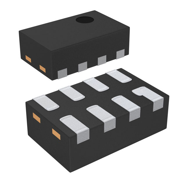
Pin Configuration
VDD
1
ON
2
D
3
D
4
Using a proprietary MOSFET design, the SLG59M1658V
achieves a stable 17 mΩ RDSON across a wide input voltage
range. In addition, the SLG59M1658V’s package also exhibits
low thermal resistance for high-current operation using
Silego’s proprietary CuFET technology.
Fully specified over the -40 °C to 125 °C temperature range,
the SLG59M1658V is packaged in a space-efficient, low
thermal resistance, RoHS-compliant 1.0 mm x 1.6 mm STDFN
package.
Features
• 1.0 x 1.6 x 0.55 mm STDFN 8L package (2 fused pins for
drain and 2 fused pins for source)
• Logic level ON pin capable of supporting 0.85 V CMOS
Logic
• User selectable ramp rate with external capacitor
• 17 mΩ RDSON while supporting 2.5 A
• Discharges load when off
• Two Over Current Protection Modes
• Short Circuit Current Limit
• Active Current Limit
• Over Temperature Protection
• Pb-Free / Halogen-Free / RoHS compliant
• Operating Temperature: -40 °C to 125°C
• Operating Voltage: 2.5 V to 5.5 V
SLG59M1658V
The SLG59M1658V is a high performance 17 mΩ, 2.5 A
single-channel nFET integrated power switch which can
operate with a 2.5 V to 5.5 V VDD supply to switch power rails
from as low as 0.9 V up to the supply voltage. The
SLG59M1658V incorporates two-level overload current
protection, thermal shutdown protection, fast output voltage
discharge, and in-rush current control which can easily be
adjusted by a small external capacitor.
8
GND
7
CAP
6
S
5
S
8-pin STDFN
(Top View)
Applications
• Notebook Power Rail Switching
• Tablet Power Rail Switching
• Smartphone Power Rail Switching
Block Diagram
2.5 A @ 17 mΩ
D
CIN
VDD
+2.5 to 5.5 V
CAP
CSLEW
4 nF
S
CLOAD
Charge
Pump
Linear Ramp
Control
Over Current and
Over Temperature
Protection
ON
CMOS Input
GND
Silego Technology, Inc.
000-0059M1658-100
Rev 1.00
Revised February 23, 2017
�SLG59M1658V
Pin Description
Pin #
Pin Name
Type
Pin Description
1
VDD
PWR
With an internal 1.8 V UVLO threshold, VDD supplies the power for the
operation of the power switch and internal control circuitry. Bypass the VDD
pin to GND with a 0.1 µF (or larger) capacitor.
2
ON
Input
A low-to-high transition on this pin initiates the operation of the
SLG59M1658V’s state machine. ON is a CMOS input with VIL < 0.25 V
and VIH > 0.85 V thresholds. While there is an internal pull-down circuit to
GND (~4 MΩ), connect this pin directly to a general-purpose output (GPO)
of a microcontroller, an application processor, or a system controller. Do
not allow this pin to be open-circuited.
3, 4
D
MOSFET
Drain terminal connection of the n-channel MOSFET (2 pins fused for VD).
Connect at least a low-ESR 0.1 µF capacitor from this pin to ground.
Capacitors used at VD should be rated at 10 V or higher.
5, 6
S
MOSFET
Source terminal connection of the n-channel MOSFET (2 pins fused for
VS). Connect a low-ESR capacitor from this pin to ground and consult the
Electrical Characteristics table for recommended CLOAD range. Capacitors
used at VS should be rated at 10 V or higher.
7
CAP
Input
A low-ESR, stable dielectric, ceramic surface-mount capacitor connected
from CAP pin to GND sets the VS slew rate and overall turn-on time of the
SLG59M1658V. For best performance CSLEW value should be ≥ 1.5 nF
and voltage level should be rated at 10 V or higher.
8
GND
GND
Ground connection. Connect this pin to system analog or power ground
plane.
Ordering Information
Part Number
Type
Production Flow
SLG59M1658V
STDFN 8L
Extended Industrial, -40 °C to 125 °C
SLG59M1658VTR
STDFN 8L (Tape and Reel)
Extended Industrial, -40 °C to 125 °C
000-0059M1658-100
Page 2 of 14
�SLG59M1658V
Absolute Maximum Ratings
Parameter
VDD
Description
Conditions
Power Supply
Min.
Typ.
Max.
Unit
--
--
7
V
VD to GND
Power Switch Input Voltage to
GND
-0.3
--
7
V
VS to GND
Power Switch Output Voltage to
GND
-0.3
--
VD
V
-0.3
--
7
V
ON and CAP to
ON and CAP Pin Voltages to GND
GND
-65
--
150
°C
ESDHBM
TS
ESD Protection
Human Body Model
2000
--
--
V
ESDCDM
ESD Protection
Charged Device Model
1000
--
--
V
MSL
θJA
WDIS
Storage Temperature
Moisture Sensitivity Level
Thermal Resistance
1
1.0 x 1.6 mm, 8L STDFN; Determined using 1 in2, 1 oz. copper pads under each VD
and VS terminals and FR4 pcb material
Package Power Dissipation
MOSFET IDS Max Continuous Switch Current
MOSFET IDSPK Peak Current from Drain to Source For no more than 1 ms with 1% duty cycle
--
74
--
°C/W
--
--
0.4
W
--
--
2.5
A
--
--
3.5
A
Note: Stresses greater than those listed under “Absolute Maximum Ratings” may cause permanent damage to the device. This is a stress rating
only and functional operation of the device at these or any other conditions above those indicated in the operational sections of this
specification is not implied. Exposure to absolute maximum rating conditions for extended periods may affect reliability.
Electrical Characteristics
TA = -40 to 125 °C (unless otherwise stated)
Parameter
VDD
VDD_UVLO
IDD
RDSON
VD
IFET_OFF
Description
Conditions
Min.
Typ.
Max.
Unit
Power Supply Voltage
-40 to 125°C
2.5
--
5.5
V
VDD Undervoltage Lockout
Threshold
VDD ↑
--
1.8
--
V
when OFF; TA = 70 °C;
VS = 0 V; VD = VDD = 5.5 V
--
--
1
μA
when OFF; TA = 85 °C;
VS = 0 V; VD = VDD = 5.5 V
--
--
1
μA
when OFF; TA = 125 °C;
VS = 0 V; VD = VDD = 5.5 V
--
--
1
μA
when ON, no Load
--
75
100
μA
Power Supply Current (PIN 1)
Static Drain to Source
ON Resistance
TA 25°C @ 100 mA
--
17
20.4
mΩ
TA 85°C @ 100 mA
--
20.5
24
mΩ
TA 125°C @ 100 mA
--
24
28.8
mΩ
0.9
--
VDD
V
VD = VDD = 5.5 V;
VS = 0 V; ON = 0 V; TA = 70°C
--
--
1
μA
VD = VDD = 5.5 V;
VS = 0 V; ON = 0 V; TA = 85°C
--
--
1
μA
VD = VDD = 5.5 V;
VS = 0 V; ON = 0 V; TA = 125°C
--
--
5
μA
Drain Voltage
MOSFET OFF Leakage Current
000-0059M1658-100
Page 3 of 14
�SLG59M1658V
Electrical Characteristics (continued)
TA = -40 to 125 °C (unless otherwise stated)
Parameter
TON_Delay
Description
Conditions
ON pin Delay Time
50% ON to Ramp Begin
Min.
--
Slew Rate
Example: CSLEW (PIN 7) = 4 nF,
VDD = VD = 5 V, CLOAD = 10 μF,
RLOAD = 20 Ω
Max.
200
--
--
3.3
V/ms
--
V/ms
Configurable 1
50% ON to 90% VS
Unit
μs
Configurable 1
10% VS to 90% VS
VS(SR)
Typ.
ms
Example: CSLEW (PIN 7) = 4 nF,
VDD = VD = 5 V, CLOAD = 10 μF,
RLOAD = 20 Ω
--
1.50
--
ms
OFF Delay Time
50% ON to VS Fall Start,
VDD = VD = 5 V, no CLOAD,
RLOAD = 20 Ω
--
8
--
μs
TFALL
VS Fall Time
90% VS to 10% VS, VDD = VD = 5 V,
no CLOAD, RLOAD = 20 Ω
--
3.3
--
μs
CLOAD
Output Load Capacitance
CLOAD connected from VS to GND
--
--
500
μF
Discharge Resistance
100
200
300
Ω
ON_VIH
High Input Voltage on ON pin
0.85
--
VDD
V
ON_VIL
Low Input Voltage on ON pin
TTotal_ON
TOFF_Delay
RDIS
Total Turn On Time
-0.3
0
0.25
V
Active Current Limit (IACL)
MOSFET will automatically limit current when VS > 250 mV
--
4.5
--
A
Short Circuit Current Limit (ISCL)
MOSFET will automatically limit current when VS < 250 mV
--
0.5
--
A
Thermal shutoff turn-on temperature
--
150
--
°C
THERMOFF Thermal shutoff turn-off temperature
--
130
--
°C
THERMTIME Thermal shutoff time
--
--
1
ms
ILIMIT
THERMON
Notes:
1. Refer to table for configuration details.
000-0059M1658-100
Page 4 of 14
�SLG59M1658V
TTotal_ON, TON_Delay and Slew Rate Measurement
ON
50% ON
50% ON
TOFF_Delay
90% VS
VS
90% VS
TON_Delay
10% VS
10% VS
VS(SR) (V/ms)
TFALL
TTotal_ON
Note: Rise and Fall times of the ON signal are 100 ns
000-0059M1658-100
Page 5 of 14
�SLG59M1658V
Typical Performance Characteristics
RDSON vs. VDD, and Temperature
RDSON vs. VD and VDD
000-0059M1658-100
Page 6 of 14
�SLG59M1658V
VS(SR)
VS(SR) vs. Temperature, VD, VDD, and CSLEW
TTotal_ON vs. CSLEW, VD, VDD, and Temperature
000-0059M1658-100
Page 7 of 14
�SLG59M1658V
Typical Operation Waveforms
ON
VS
Figure 1. Typical Turn ON operation waveform for VDD = VD = 5 V, CSLEW = 4 nF, CLOAD = 10 µF, RLOAD = 20 Ω
ON
VS
Figure 2. Typical Turn ON operation waveform for VDD = VD = 5 V, CSLEW = 12 nF, CLOAD = 10 µF, RLOAD = 20 Ω
000-0059M1658-100
Page 8 of 14
�SLG59M1658V
ON
VS
Figure 3. Typical Turn OFF operation waveform for VDD = VD = 5 V, CSLEW = 4 nF, no CLOAD, RLOAD = 20 Ω
ON
VS
Figure 4. Typical Turn OFF operation waveform for VDD = VD = 5 V, CSLEW = 4 nF, CLOAD = 10 µF, RLOAD = 20 Ω
000-0059M1658-100
Page 9 of 14
�SLG59M1658V
SLG59M1658V Power-Up/Power-Down Sequence Considerations
To ensure glitch-free power-up under all conditions, apply VDD first, followed by VD after VDD exceeds 1 V. Then allow VD to reach
90% of its max value before toggling the ON pin from Low-to-High. Likewise, power-down in reverse order.
If VDD and VD need to be powered up simultaneously, glitching can be minimized by having a suitable load capacitor. A 10 μF
CLOAD will prevent glitches for rise times of VDD and VD less than 2 ms.
If the ON pin is toggled HIGH before VDD and VD have reached their steady-state values, the IPS timing parameters may differ
from datasheet specifications.
The slew rate of output VS follows a linear ramp set by a capacitor connected to the CAP pin. A larger capacitor value at the CAP
pin produces a slower ramp, reducing inrush current from capacitive loads.
SLG59M1658V Current Limiting
The SLG59M1658V has two modes of current limiting, differentiated by the output (Source pin) voltage.
1. Standard Current Limiting Mode (with Thermal Protection)
When V(S) > 250 mV, the output current is initially limited to the Active Current Limit specification given in the Electrical Characteristics table. The current limiting circuit is very fast and responds within a few micro-seconds to sudden loads. When overload
is sensed, the current limiting circuit increases the FET resistance to keep the current from exceedng the Active Current Limit.
However, if an overload condition persists, the die temperature rise due to the increased FET resistance while at maximum current
can activate Thermal Protection. If the die temperature exceeds the THERMON specification, the FET is shut completely OFF,
allowing the die to cool. When the die cools to the THERMOFF temperature, the FET is allowed to turn back on. This process may
repeat as long as the overload condition is present.
2. Short Circuit Current Limiting Mode (with Thermal Protection)
When V(S) < 250 mV (which is the case with a hard short, such as a solder bridge on the power rail), the current is limited to
approximately 500 mA. Thermal Protection is also present, but since the Short Circuit Current Limit is much lower than Standard
Current Limit, activation may only occur at higher ambient temperatures.
For more information on Silego GreenFET3 integrated power switch features, please visit our Application Notes page at our
website and see App Note “AN-1068 GreenFET3 Integrated Power Switch Basics”.
000-0059M1658-100
Page 10 of 14
�SLG59M1658V
Package Top Marking System Definition
ABC
Serial Number
Pin 1 Identifier
ABC - Part Serial Number Field
each A, B, and C character can be A-Z and 0-9
000-0059M1658-100
Page 11 of 14
�SLG59M1658V
Package Drawing and Dimensions
8 Lead STDFN Package 1.0 x 1.6 mm (Fused Lead)
000-0059M1658-100
Page 12 of 14
�SLG59M1658V
Tape and Reel Specifications
Max Units
Leader (min)
Nominal
Reel &
Package # of
Package Size
Hub Size
Length
Type
Pins
per Reel per Box
Pockets
[mm]
[mm]
[mm]
STDFN 8L
1x1.6mm
0.4P FC
Green
8
1.0 x 1.6 x 0.55
3,000
3,000
178 / 60
100
400
Trailer (min)
Pockets
Length
[mm]
Tape
Width
[mm]
100
400
8
Part
Pitch
[mm]
4
Carrier Tape Drawing and Dimensions
Pocket BTM Pocket BTM
Package
Length
Width
Type
STDFN 8L
1x1.6mm
0.4P FC
Green
Pocket
Depth
Index Hole
Pitch
Pocket
Pitch
Index Hole
Diameter
Index Hole Index Hole
to Tape
to Pocket Tape Width
Edge
Center
A0
B0
K0
P0
P1
D0
E
F
W
1.12
1.72
0.7
4
4
1.55
1.75
3.5
8
Recommended Reflow Soldering Profile
Please see IPC/JEDEC J-STD-020: latest revision for reflow profile based on package volume of 0.88 mm3 (nominal). More
information can be found at www.jedec.org.
000-0059M1658-100
Page 13 of 14
�SLG59M1658V
Revision History
Date
Version
2/23/2017
1.00
000-0059M1658-100
Change
Production Release
Page 14 of 14
�