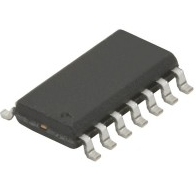
TF2190(4)M
High-Side and Low-Side Gate Driver
Features
Description
F
� loating high-side driver in bootstrap operation to 600V
�Drives two N-channel MOSFETs or IGBTs in a half-bridge
configuration
Output drivers capable of 4.5A/4.5A typ sink/source
Logic input (HIN and LIN) 3.3V capability
Schmitt triggered logic inputs with internal pulldown
Undervoltage lockout for high and low-side drivers
Extended temperature range: -40°C to +125°C
The TF2190M is a high voltage, high speed gate driver
capable of driving N-channel MOSFET’s and IGBTs in a
half-bridge configuration. TF Semi’s high voltage process
enables the TF2190M’s high side to switch to 600V in a
bootstrap operation under high dV/dt conditions.
The TF2190M logic inputs are compatible with standard
TTL and CMOS levels (down to 3.3V) to interface easily
with controlling devices. The driver outputs feature high
pulse current buffers designed for minimum driver cross
conduction.
The TF2190M is offered in space saving 8-pin SOIC and
the TF21904M in the 14-pin SOIC and operates over an
extended -40°C to +125°C temperature range.
Applications
Motor Controls
DC-DC Converters
AC-DC Inverters
Class D Power Amplifiers
SOIC-14(N)
SOIC-8(N)
Ordering Information
Typical Application
PART NUMBER PACKAGE
PACK / Qty
TF2190M-TAH
T&R / 2500
SOIC-8(N)
TF21904M-TUH SOIC-14(N)
T&R / 2500
Year Year Week Week
MARK
YYWW
TF2190M
Lot ID
YYWW
TF21904M
Lot ID
Up to 600V
HIN
HIN
VB
LIN
LIN
HO
COM
R4
LO
www.tfsemi.com
Jun. 2021
TF2190M
VS
VCC
TO
LOAD
VCC
Rev 1.4
1
�Advance Info
TF2190(4)M
High-Side and Low-Side Gate Driver
Pin Diagrams
HIN
1
8
HIN
1
14
NC
VB
LIN
2
13
VB
VSS
3
12
HO
NC
4
11
VS
COM
5
10
NC
LO
6
9
NC
VCC
7
8
NC
LIN
2
7
HO
COM
3
6
VS
LO
4
5
VCC
Top View: SOIC-8(N), TF2190M
Top View: SOIC-14(N), TF21904M
Pin Descriptions
PIN NAME
PIN DESCRIPTION
HIN
Logic input for high-side gate driver output, in phase with HO
LIN
Logic input for low-side gate driver output, in phase with LO
COM
Low-side and logic return
LO
Low-side gate drive output
VCC
Low-side and logic fixed supply
VS
High-side floating supply return
HO
High-side gate driver output
VB
High-side floating supply
VSS
Logic Ground (TF21904M only)
Jun. 2021
2
�Advance Info
TF2190(4)M
High-Side and Low-Side Gate Driver
Functional Block Diagrams
VCC
Vcc
TF2190M
VB
UV
Detect
UV
Detect
R
HIN
Pulse
Gen
HV Level
Shift
Q
HO
R
S
High Voltage Well
Vs
VCC
LIN
LO
Delay
COM
VCC
Vcc
TF21904M
VB
UV
Detect
UV
Detect
R
HIN
Pulse
Gen
HV Level
Shift
Q
HO
R
S
High Voltage Well
Vs
VCC
LIN
VSS
Jun. 2021
VSS/COM
Level
Shift
Delay
LO
COM
3
�Advance Info
TF2190(4)M
High-Side and Low-Side Gate Driver
Absolute Maximum Ratings (NOTE1)
A
VB - High side floating supply voltage...............-0.3V to +624V
VS - High side floating supply offset voltage....VB -24V to VB+0.3V
VSS - Logic Supply offset voltage.........................VCC -24V to VCC + 0.3V
VHO - High side floating output voltage...............VS-0.3V to VB+0.3V
dVS / dt - Offset supply voltage transient...............................50 V/ns
PD - Package power dissipation at TA ≤ 25 °C
SOIC-8.............................................................................................0.625W
SOIC-14...........................................................................................0.862W
VCC - Low side and logic fixed supply voltage..............-0.3V to +24V
VLO - Low side output voltage..................................-0.3V to VCC+0.3V
VIN - Logic input voltage (HIN and LIN)... -0.3V to VCC+0.3V
NOTE1 Stresses beyond those listed under “Absolute Maximum Ratings” may cause
permanent damage to the device. These are stress ratings only, and functional operation
of the device at these or any other conditions beyond those indicated in the operational
sections of the specifications is not implied. Exposure to absolute maximum rating
conditions for extended periods may affect device reliability.
SOIC-8 Thermal Resistance (NOTE2)
qJC..................................................................................................45 °C/W
qJA ...............................................................................................200 °C/W
SOIC-14 Thermal Resistance (NOTE2)
qJA ................................................................................................145 °C/W
TJ - Junction operating temperature .......................................+150 °C
TL - Lead temperature (soldering, 10s) .................................. +300 °C
Tstg - Storage temperature range ............................-55 °C to +150 °C
NOTE2 When mounted on a standard JEDEC 2-layer FR-4 board.
Recommended Operating Conditions
Symbol
Parameter
MIN
MAX
VB
High side floating supply absolute voltage
VS + 10
VS + 20
VS
High side floating supply offset voltage
NOTE3
600
VSS
Logic ground (TF21904 only)
-5
5
VHO
High side floating output voltage
VS
VB
VCC
Low side fixed supply voltage
10
20
VLO
Low side output voltage
0
VCC
VIN
Logic input voltage (HIN and LIN)
0
5
TA
Ambient temperature
-40
125
Unit
V
°C
NOTE3 Logic operational for VS of -5V to +600V.
Jun. 2021
4
�Advance Info
TF2190(4)M
High-Side and Low-Side Gate Driver
DC Electrical Characteristics (NOTE4)
VBIAS (VCC, VBS ) = 15V, TA = 25 °C , unless otherwise specified.
Symbol
Parameter
VIH
Logic “1” input voltage
VIL
Logic “0” input voltage
VCC = 10V to 20V
NOTE5
VOH
High level output voltage, VBIAS - VO
IO = 0mA
0.1
VOL
Low level output voltage, VO
IO = 0mA
0.035
ILK
Offset supply leakage current
VB = VS = 600V
IBSQ
Quiescent VBS supply current
VIN = 0V or 5V
45
80
ICCQ
Quiescent VCC supply current
VIN = 0V or 5V
75
200
IIN+
Logic “1” input bias current
VIN = 5V
25
50
IIN-
Logic “0” input bias current
VIN = 0V
1.0
2.0
VBSUV+
VBS supply under-voltage positive going
threshold
7.6
8.4
9.8
VBSUV-
VBS supply under-voltage negative going
threshold
6.9
7.8
9.0
VCCUV+
VCC supply under-voltage positive going
threshold
7.6
8.4
9.8
VBSUV-
VCC supply under-voltage negative going
threshold
6.9
7.8
9.0
VCCUVH
VBSUVH
Conditions
MIN
Output high short circuit pulsed current
IO-
Output low short circuit pulsed current
MAX
Unit
2.5
0.8
V
50
VCC and VBS under-voltage hysteresis
IO+
TYP
mA
V
0.6
VO = 0V, PW ≤ 10 ms
3.5
4.5
A
3.5
4.5
NOTE4 The VIN, VTH, and IIN parameters are applicable to the two logic input pins: HIN and LIN. The VO and IO parameters are applicable to the respective output pins: HO and LONOTE5 For optimal operation, it is highly recommended that the input pulse (to HIN and LIN) should have an amplitude of 2.5V minimum with a pulse width of 280ns minimum.
Jun. 2021
VO = 15V, PW ≤ 10 ms
5
�Advance Info
TF2190(4)M
High-Side and Low-Side Gate Driver
AC Electrical Characteristics
VBIAS (VCC, VBS ) = 15V, CL = 1000pF, and TA = 25 °C , unless otherwise specified.
Symbol
Parameter
Conditions
ton
Turn-on propogation delay
toff
Turn-off propogation delay
tDM
Delay matching, HS & LS turn on/off
tr
Turn-on rise time
tf
Turn-off fall time
MIN
TYP
MAX
VS = 0V
140
200
VS = 0V
140
200
0
50
25
50
20
45
VS = 0V
Unit
ns
Timing Waveforms
HIN
50%
LIN
HIN
LIN
50%
LO
HO
10%
HO
LO
tDM
tDM
90%
LO
Figure 1. Input / Output Timing Diagram
HIN
LIN
Figure 2. Delay Matching Waveform Definitions
50%
tON
HO
LO
HO
50%
tr
tOFF
90%
90%
10%
tf
10%
Figure 3. Switching Time Waveform Definitions
Jun. 2021
6
�Advance Info
TF2190(4)M
High-Side and Low-Side Gate Driver
Application Information
RB1
12V
CV1
CV2
400V from PFC
DB1
VCC
VB
HIN
HO
TF2190M
LIN
COM
CB1
RRG1
CHV1
DRG1
CHV2
Q1
RG1
VS
RRG2 DRG2
LO
Q2
MCU/
Control
RG2
RB2
CV3
DB2
VCC
VB
HIN
HO
LIN
COM
TF2190M
VS
CB1
RRG3
DRG3
CHV3
Q3
RG3
RRG4 DRG4
LO
Q4
RG4
Figure 4. Primary side of Full Bridge converter using TF2190
RRG1, RRG2, RRG3, and RRG4 values are typically between 0Ω and 10Ω, exact value decided
by MOSFET junction capacitance and drive current of gate driver; 10Ω is used in this example.
It is highly recommended that the input pulse (to HIN and LIN) should have an amplitude of 2.
5V minimum (for VDD=15V) with a minimum pulse width of 280ns
RG1, RG2, RG3, and RG4 values are typically between 20Ω and 100Ω, exact value decided by MOSFET
junction capacitance and drive current of gate driver; 50Ω is used in this example.
RB1 and RB2 value is typically between 3Ω and 20Ω, exact value depending on bootstrap capacitor
value and amount of current limiting required for bootstrap capacitor charging; 10Ω is used in this
example. Also DB1 and DB2 should be an ultra fast diode of 1A rating minimum and voltage rating
greater than system operating voltage.
.
Jun. 2021
7
�Advance Info
TF2190(4)M
High-Side and Low-Side Gate Driver
150
140
130
ton High Side
120
ton Low Side
Turn On Propagation Delay (ns)
Turn On Propagation Delay (ns)
150
110
100
90
80
70
60
50
10
12
14
16
18
140
130
120
110
100
90
80
ton High Side
70
ton Low Side
60
50
20
-40
-20
0
Supply Voltage (V)
140
140
Turn Off Propagation Delay (ns)
Turn Off Propagation Delay (ns)
150
130
120
110
100
90
70
toff Low Side
60
50
10
12
14
16
18
100
120
120
110
100
90
80
toff High Side
70
toff Low Side
60
50
20
-40
-20
0
20
40
60
80
100
120
Temperature (°C)
Figure 7. Turn-off Propagation Delay vs. Supply Voltage
Figure 8. Turn-off Propagation Delay vs. Temperature
40
40
35
35
tr High Side
30
25
20
15
20
15
10
5
5
0
12
14
16
18
Supply Voltage (V)
Figure 9. Rise Time vs. Supply Voltage
20
tr Low Side
25
10
10
tr High Side
30
tr Low Side
Rise Time (ns)
Rise Time (ns)
80
130
Supply Voltage (V)
Jun. 2021
60
Figure 6. Turn-on Propagation Delay vs. Temperature
150
toff High Side
40
Temperature (°C)
Figure 5. Turn-on Propagation Delay vs. Supply Voltage
80
20
0
-40
-20
0
20
40
60
80
100
120
Temperature (°C)
Figure 10. Rise Time vs. Temperature
8
�Advance Info
TF2190(4)M
High-Side and Low-Side Gate Driver
40
40
35
35
tf High Side
tf Low Side
25
20
15
20
15
10
5
5
0
12
14
16
18
tf Low Side
25
10
10
tf High Side
30
Fall Time (ns)
Fall Time (ns)
30
0
20
-40
-20
0
20
Supply Voltage (V)
100
120
5.0
4.5
tdmon
4.5
4.0
tdmoff
4.0
Delay Matching (ns)
Delay Matching (ns)
80
Figure 12. Fall Time vs. Temperature
5.0
3.5
3.0
2.5
2.0
1.5
1.0
0.5
3.5
3.0
2.5
2.0
1.5
tdmon
1.0
tdmoff
0.5
0.0
10
12
14
16
18
0.0
20
-40
-20
0
20
40
60
80
100
120
Temperature (°C)
Supply Voltage (V)
Figure 14. Delay Matching vs. Temperature
Figure 13. Delay Matching vs. Supply Voltage
10.0
10.0
9.0
9.0
IO+ High Side
8.0
8.0
IO+ High Side
7.0
Output Source Current (A)
Output Source Current (A)
60
Temperature (°C)
Figure 11. Fall Time vs. Supply Voltage
IO+ Low Side
6.0
5.0
4.0
3.0
2.0
1.0
0.0
IO+ Low Side
7.0
6.0
5.0
4.0
3.0
2.0
1.0
0.0
10
12
14
16
18
20
Supply Voltage (V)
Figure 15. Output Source Current vs. Supply Voltage
Jun. 2021
40
-40
-20
0
20
40
60
80
100
120
Temperature (°C)
Figure 16. Output Source Current vs. Temperature
9
�Advance Info
TF2190(4)M
High-Side and Low-Side Gate Driver
10.0
10.0
9.0
9.0
IO- High Side
7.0
Output Sink Current (A)
Output Sink Current (A)
8.0
IO- Low Side
6.0
5.0
4.0
3.0
2.0
1.0
IO- High Side
8.0
IO- Low Side
7.0
6.0
5.0
4.0
3.0
2.0
1.0
0.0
10
12
14
16
18
0.0
20
-40
-20
0
20
Supply Voltage (V)
140
ICCq
Quiescent Current (µ
µA)
Quiescent Current (µ
µA)
IBSq
120
100
80
60
40
160
IBSq
140
ICCq
120
100
20
80
60
40
20
0
10
12
14
16
18
0
20
-40
-20
0
Supply Voltage (V)
160
IBSq
140
ICCq
120
100
0.8
80
VIH High Side
0.6
60
VIH Low Side
40
20
0.0
10
100
120
1.6
1.4
1.2
1.0
0.8
VIH High Side
0.6
VIH Low Side
0.4
0.2
0.0
0
10
12
12
14 14
16 16
18 18
2020
Supply
Voltage
(V)(V)
Supply
Voltage
Figure 21. Logic 1 Input Voltage vs. Supply Voltage
Jun. 2021
80
1.8
180
0.2
60
2.0
200
0.4
40
Figure 20. Quiescent Current vs. Temperature
Logic 1 Input Voltage (V)
Quiescent Current (µ
µA)
Logic 1 Input Voltage (V)
1.0
20
Temperature (°C)
Figure 19. Quiescent Current vs. Supply Voltage
1.2
120
180
160
1.4
100
200
180
1.6
80
Figure 18. Output Sink Current vs. Temperature
200
1.8
60
Temperature (°C)
Figure 17. Output Sink Current vs. Supply Voltage
2.0
40
-40
-20
0
20
40
60
80
100
120
Temperature (°C)
Figure 22. Logic 1 Input Voltage vs. Temperature
10
�Advance Info
TF2190(4)M
High-Side and Low-Side Gate Driver
2.0
2.0
1.8
Logic 0 Input Voltage (V)
1.8
Logic 0 Input Voltage (V)
1.6
1.4
1.2
1.0
0.8
VIL High Side
0.6
VIL Low Side
0.4
1.6
1.4
1.2
1.0
0.8
VIL High Side
0.6
VIL Low Side
0.4
0.2
0.2
0.0
0.0
10
12
14
16
18
-40
20
-20
0
16
16
14
14
12
12
10
8
6
VCCUV+
0
0
20
40
100
120
8
6
VBSUV+
VBSUV-
2
-20
80
10
4
VCCUV-
-40
60
Figure 24. Logic 0 Input Voltage vs. Temperature
VBS UVLO (V)
VCC UVLO (V)
Figure 23. Logic 0 Input Voltage vs. Supply Voltage
2
40
Temperature (°C)
Supply Voltage (V)
4
20
60
80
100
120
Temperature (°C)
0
-40
-20
0
20
40
60
80
100
120
Temperature (°C)
Figure 25. VCC UVLO vs. Temperature
Figure 26. VBS UVLO vs. Temperature
Offset Supply Leakage Current (µ
µA)
20.0
18.0
16.0
14.0
12.0
10.0
8.0
6.0
4.0
2.0
0.0
-40
-20
0
20
40
60
80
100
120
Temperature (°C)
Figure 27. Offset Supply Leakage Current Temperature,
VB=VS= 600V
Jun. 2021
11
�Advance Info
TF2190(4)M
High-Side and Low-Side Gate Driver
Operation
Halfbridge Configuration
A common configuration used for the TF2190 is a halfbridge (see fig. 29). In a half-bridge configuration the
source of the high-side MOSFET (QH) and the drain of the
low-side MOSFET (QL) are connected. That line (VS) is both
the return for the high side in the gate driver IC as well
as the output of the half-bridge. When QH is on and QL is
off, VS swings to high voltage, and when QH is off and QL
is on, VS swings to GND. Hence the output switches from
GND to high voltage at the frequency of HIN and LIN, this
line drives a transformer for a power supply, or a coil on a
motor.
In this half-bridge configuration, high voltage DC is input
to the MOSFETs, and converted to a high voltage switching
signal to output to load (fig 29). The MOSFETs operate
in saturation mode and an important function of the
gate driver is to turn on the MOSFET quickly to minimize
switching losses from the linear region of the MOSFET
(turn on and turn off); the TF2190 has a typical rise/fall time
of 25ns/20ns into a 1nF load.
Another important function of the gate driver IC in the
half-bridge configuration is to convert the logic signals
of control (TF2190 operates at logic 3V), to a voltage level
and current capacity to drive the gate of the MOSFET and
IGBT; this requires driving large currents initially to turn on/
turn off the MOSFET quickly. Also the floating well of the
high-side allows high voltage operation in the bootstrap
operation.
VHV
CHV
RGH
HIN
HIN
LIN
LIN
R4
VB
TF2190
QH
CB
VS
HO
COM
VS
LO
VCC
VCC
CD
RGL
QL
Figure 29. TF2190 in a half-bridge configuration
Bootstrap Operation
The supply for the TF2190 High Side is provided by the
bootstrap capacitor CB (see fig 30). In the half-bridge
configuration, VS swings from 0V to VHV depending on the
PWM input ot the IC. When VS is 0V, VBS will go below VCC
and VCC will charge CB . When HO goes high, VS swings to
VHV , and VBS remains at VCC minus a diode drop (DB) due
to the voltage on CB . This is the supply for the high side
gate driver and allows the gate driver to function with the
floating well (VS ) at the high voltage.
When considering the value of the bootstrap capacitor
CB , it is important that it is sized to provide enough
energy to quickly drive the gate of QH . Values of 1mF to
10mF are recommended, exact value depending on gate
capacitance, and the noise in application. It is key to use a
low ESR capacitor that is close to the device. This will best
quickly supply charge to the gate of the MOSFET.
Jun. 2021
VCC
DB
HV
VB
Gate Driver IC
High Side
CB
QH
HO
RGH
VS
Figure 30. TF2190 high side in bootstrap operation
12
�Advance Info
TF2190(4)M
High-Side and Low-Side Gate Driver
For a more detailed description on Gate Resistor Selection and Bootstrap Capacitor Selectrion, see the TF
Semiconductor’s High Voltage Gate Driver Application Note (AN1347).
Gate Drive Control
The most crucial time in the gate drive is the turn on and
turn off of the MOSFET, and performing this function
quickly, but with minimal noise and ringing is key. Too fast
a rise/fall time can cause unnecessary ringing, and too slow
a rise/fall time will increase switching losses in the MOSFET.
An example of just the high side gate driver is shown in
figure 31 (any selection of gate driver components should
be the same for high side and low side drive); two extra
components are seen, RDH and DH. With the careful selection of
RGH and RDH , it is possible to selectively control the rise time
and fall time of the gate drive. For turn on, all current will
go from the IC through RGH and charge the MOSFET gate
capacitor, hence increasing or decreasing RGH will increase
or decrease rise time in the application. With the addition
of DH , the fall time can be separately controlled as the turn
off current flows from the MOSFET gate capacitor, through
DH and RDH to the driver in the IC to VS. So increasing or
decreasing RDH will increase or decrease the fall time.
Increasing turn on and turn off has the effect of limiting
ringing and noise due to parasitic inductances, hence
with a noisy environment, it may be necessary to
increase the gate resistors. For gate resistor value
selection the exact value depends on the type of
application, level of noise and ringing expected, and
EMI requirements. Generally, power supplies switch at
a fast speed, and want to squeeze out efficiency of the
MOSFETs, so lower values are recommended, for example
RGH = 5W - 20W. For motors, the switching speed is
generally slower, and the application has more inherent
noise, so higher values are recommended, for example
RGH = 20W - 100W.
VCC
VB
TF2190
HO
RDH
DH
QH
RGH
VS
OUT
Figure 31. Gate Drive Control
Jun. 2021
13
�Advance Info
TF2190(4)M
High-Side and Low-Side Gate Driver
Application Information
Layout Considerations
Layout plays a considerable role in noise and ringing
in a circuit; unwanted noise coupling, unpredicted
glitches and abnormal operation could arise due to
poor layout of the associated components. Figure 31
shows a halfbridge schematic with parasitic inductances
in the high current path (LP1, LP2, LP3, LP4) which would
be caused by inductance in the metal of the trace.
Considering fig. 32, the length of the tracks in red
should be minimized, and the bootstrap capacitor (CB)
and the decoupling capacitor (CD) should be placed as
close to the IC as possible. Low ESR ceramic capacitors
should be used to minimize inductance. And finally the
gate resistors (RGH and RGL) and the sense resistor (RS)
should be surface mount devices. These suggestions
will reduce the parasitics due to the PCB traces.
Generally, for the decoupling capacitor (CD), at least
one low ESR capacitor is recommended close to the VCC
pin. Recommended values are 1mF to 10mF. A second
smaller decoupling capacitor in parallel is sometimes
added to provide better high frequency response (for
example 0.1mF).
RGH
CHV
HO
VB
VS
VCC
CB
VCC
Minimize area
LP1
LP2
CD
Keep high voltage and
high current line away
from logic and analog
lines
RGL
LO
COM
LP3
RS
LP4
Figure 32. Layout Suggestions for TF2190 in a halfbridge
Jun. 2021
14
�Advance Info
TF2190(4)M
High-Side and Low-Side Gate Driver
Application Example
400V
50R
HIN
HIN
LIN
LIN
R4
2.2 F
VB
TF2190
HO
COM
VS
LO
VCC
VCC
2.2 F
50R
50R
HIN
HIN
LIN
LIN
R4
2.2 F
VB
TF2190
M
HO
COM
VS
LO
VCC
VCC
2.2 F
50R
400V
1000W
PMSM
50R
HIN
HIN
LIN
LIN
R4
VB
TF2190
2.2 F
HO
COM
VS
LO
VCC
VCC
2.2 F
50R
Figure 33. Three Phase Motor Driver using the TF2190
Jun. 2021
15
�Advance Info
TF2190(4)M
High-Side and Low-Side Gate Driver
VHV
HIN
To
MCU
LIN
R4
VB
TF2190
2.2 F
VS
LO
VCC
VCC
2.2 F
To
MCU
LIN
R4
VB
TF2190
5k
HO
COM
HIN
10R
2.2 F
10R
10R
5k
5k
HO
COM
VS
LO
VCC
VCC
2.2 F
10R
5k
Figure 34. The TF2190 full bridge configuration for 1kW - 3kW power supply
Jun. 2021
16
�Advance Info
TF2190(4)M
Package Dimensions (SOIC-8 N)
High-Side and Low-Side Gate Driver
Please contact support@tfsemi.com for package availability.
Jun. 2021
17
�Advance Info
TF2190(4)M
Package Dimensions (SOIC-14)
High-Side and Low-Side Gate Driver
Please contact support@tfsemi.com for package availability.
Jun. 2021
18
�Advance Info
TF2190(4)M
High-Side and Low-Side Gate Driver
Revision History
Rev.
Change
Owner
Date
1.0
First release, final datasheet
Keith Spaulding
5/20/2016
1.1
Text edit
Keith Spaulding
11/24/2017
1.2
Add Note 5
Duke Walton
7/30/2019
1.3
Add Applications information, pg 7.
Keith Spaulding
2/2/2021
1.4
Application notes update
Raj Selvaraj
06/22/2021
Important Notice
TF Semiconductor Solutions (TFSS) PRODUCTS ARE NEITHER DESIGNED NOR INTENDED FOR USE IN MILITARY AND/OR
AEROSPACE, AUTOMOTIVE OR MEDICAL DEVICES OR SYSTEMS UNLESS THE SPECIFIC TFSS PRODUCTS ARE SPECIFICALLY
DESIGNATED BY TFSS FOR SUCH USE. BUYERS ACKNOWLEDGE AND AGREE THAT ANY SUCH USE OF TFSS PRODUCTS WHICH TFSS
HAS NOT DESIGNATED FOR USE IN MILITARY AND/OR AEROSPACE, AUTOMOTIVE OR MEDICAL DEVICES OR SYSTEMS IS SOLELY AT
THE BUYER’S RISK.
TFSS assumes no liability for application assistance or customer product design. Customers are responsible for their products and
applications using TFSS products.
Resale of TFSS products or services with statements different from or beyond the parameters stated by TFSS for that product or
service voids all express and any implied warranties for the associated TFSS product or service. TFSS is not responsible or liable for
any such statements.
©2021 TFSS. All Rights Reserved. Information and data in this document are owned by TFSS wholly and may not be edited
, reproduced, or redistributed in any way without the express written consent from TFSS.
For additional information please contact support@tfsemi.com or visit www.tfsemi.com
Jun. 2021
19
�