Advance Info
TF2104M
Half-Bridge Gate Driver
Features
Description
Floating high-side driver in bootstrap operation to 600V
Drives two N-channel MOSFETs or IGBTs in a half bridge
configuration
Designed for enhanced performance in noisy motor
applications
290mA source/600mA sink output current capability
Outputs tolerant to negative transients
Internal dead time to protect MOSFETs
Wide low side gate driver supply voltage: 10V to 20V
Logic input (IN and SD*) 3.3V capability
Schmitt triggered logic inputs
Undervoltage lockout for VCC (logic and low side supply)
Extended temperature range: -40°C to +125°C
The TF2104M is a high voltage, high speed gate driver
capable of driving N-channel MOSFETs and IGBTs in a
half bridge configuration. TF Semi’s high voltage process
enables the TF2104M’s high side to switch to 600V in a
bootstrap operation.
�
�
The TF2104M logic inputs are compatible with standard
TTL and CMOS levels (down to 3.3V) to interface easily
with controlling devices. The driver outputs feature high
pulse current buffers designed for minimum driver cross
conduction.
The TF2104M is offered in PDIP-8 and SOIC-8(N) packages
and operate over an extended -40 °C to +125 °C temperature
range.
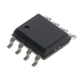
SOIC-8(N)
Applications
PDIP-8
Motor Controls
DC-DC Converters
AC-DC Inverters
Motor Drives
Ordering Information
Typical Application
Up to 600V
VCC
VCC
IN
IN
SD*
SD*
R4
COM
www.tfsemi.com
Jul 2019
VB
HO
TF2104M
PART NUMBER PACKAGE
PACK / Qty
TF2104M-3AS
PDIP-8
Tube / 50
TF2104M-TAU
SOIC-8(N)
Tube / 100
TF2104M-TAH
SOIC-8(N)
T&R / 2500
Year Year Week Week
MARK
YYWW
TF2104M
Lot ID
YYWW
TF2104M
Lot ID
TO
LOAD
VS
LO
Rev. 1.3
1
�Advance Info
TF2104M
Half-Bridge Gate Driver
Pin Diagrams
VCC
1
8
VB
IN
2
7
HO
SD*
3
6
VS
COM
4
5
LO
Top View: PDIP-8, SOIC-8
TF2104M
Pin Descriptions
PIN NAME
PIN NUMBER
PIN DESCRIPTION
VCC
1
Logic and low side supply
IN
2
Logic input for high-side and low-side gate driver outputs (HO and LO), in phase with HO
SD*
3
Logic input for shutdown, enabled low
COM
4
Low-side and logic return
LO
5
Low-side gate drive output
VS
6
High-side floating supply return
HO
7
High-side gate drive output
VB
8
High-side floating supply
Functional Block Diagram
VCC
Vcc
TF2104M
VB
UV
Detect
IN
UV
Detect
Pulse
Gen
Dead
time
HV Level
Shift/
Pulse
Filter
R
Q
HO
R
S
High Voltage Well
Vs
VCC
SD*
Delay
LO
COM
Jul 2019
2
�Advance Info
TF2104M
Half-Bridge Gate Driver
Absolute Maximum Ratings (NOTE1)
A
VB - High side floating supply voltage......................-0.3V to +624V
VS - High side floating supply offset voltage....VB -24V to VB+0.3V
VHO - High side floating output voltage...................VS-0.3V to VB+0.3V
dVS / dt - Offset supply voltage transient...................................50 V/ns
PD - Package power dissipation at TA ≤ 25 °C
SOIC-8.............................................................................................0.625W
PDIP-8...................................................................................................1.0W
VCC - Low-side fixed supply voltage...............................-0.3V to +24V
VLO - Low-side output voltage....................................-0.3V to VCC +0.3V
VIN - Logic input voltage (IN and SD*)..................-0.3V to VCC +0.3V
NOTE1 Stresses beyond those listed under “Absolute Maximum Ratings” may cause
permanent damage to the device. These are stress ratings only, and functional operation
of the device at these or any other conditions beyond those indicated in the operational
sections of the specifications is not implied. Exposure to absolute maximum rating
conditions for extended periods may affect device reliability.
SOIC-8(N) Thermal Resistance (NOTE2)
qJA ...............................................................................................200 °C/W
PDIP-8 Thermal Resistance (NOTE2)
qJA ................................................................................................125 °C/W
TJ - Junction operating temperature........................................+150 °C
TL - Lead Temperature (soldering, 10 seconds).......................+300 °C
Tstg - Storage temerature ......................................................-55 to 150 °C
NOTE2 Thermal resistance and power dissipation ratings are measured under board
mounted and still air conditions.
Recommended Operating Conditions
Symbol
Parameter
MIN
MAX
Unit
VB
High side floating supply absolute voltage
VS + 10
VS + 20
V
VS
High side floating supply offset voltage
NOTE3
600
V
VHO
High side floating output voltage
VS
VB
V
VCC
Low side fixed supply voltage
10
20
V
VLO
Low side output voltage
0
VCC
V
VIN
Logic input voltage (IN and SD*)
0
5
V
TA
Ambient temperature
-40
125
°C
NOTE3 Logic operational for VS of -5V to +600V. Logic state held for VS of -5V to -VBS
Jul 2019
3
�Advance Info
TF2104M
Half-Bridge Gate Driver
DC Electrical Characteristics (NOTE4)
VBIAS (VCC, VBS ) = 15V, TA = 25 °C , unless otherwise specified.
Symbol
Parameter
VIH
Logic “1” (IN) & Logic “0” (SD*) input voltage
VIL
Logic “0” (IN) & Logic “1” (SD*) input voltage
VOH
High level output voltage, VBIAS - VO
IO = 2mA
0.05
0.2
VOL
Low level output voltage, VO
IO = 2mA
0.02
0.1
ILK
Offset supply leakage current
VB = VS = 600V
IBSQ
Quiescent VBS supply current
VIN = 0V or 5V
60
100
ICCQ1
Quiescent VCC supply current
IN =0V or 5V, SD*=5V
350
500
ICCQ2
Quiescent VCC supply current in shutdown
IN=0V or 5V, SD*=0V
590
750
IIN+
Logic “1” input bias current
IN = 5V, SD* = 0V
3
10
IIN-
Logic “0” input bias current
IN = 0V, SD* = 5V
VCCUV+
VCC supply under-voltage positive going
threshold
8.0
8.9
9.8
VCCUV-
VCC supply under-voltage negative going
threshold
7.4
8.2
9.0
VBSUV+
VBS supply under-voltage positive going
threshold
4.5
5.5
6.5
V
VBSUV-
VBS supply under-voltage negative going
threshold
4.2
5.2
6.2
V
IO+
Output high short circuit pulsed current
VO = 0V, PW ≤ 10 ms
130
290
IO-
Output low short circuit pulsed current
VO = 15V, PW ≤ 10 ms
270
600
Conditions
MIN
VCC = 10V to 20V
2.5
TYP
NOTE5
MAX
Unit
0.8
V
50
mA
5
V
mA
NOTE4 The VIN, VTH, and IIN parameters are applicable to the two logic input pins: IN and SD*. The VO and IO parameters are applicable to the respective output pins: HO and LO
NOTE5 For optimal operation, it is recommended that the input pulse (to IN and SD*) should have an amplitude of 2.5V minimum with a pulse
width of 840ns minimum
Jul 2019
4
�Advance Info
TF2104M
Half-Bridge Gate Driver
AC Electrical Characteristics
VBIAS (VCC, VBS ) = 15V, CL = 1000pF, and TA = 25 °C , unless otherwise specified.
Symbol
Parameter
Conditions
ton
Turn-on propagation delay
toff
Turn-off propagation delay
tSD
Shutdown propagation delay
tDM
Delay matching, HS & LS turn-on/turn-off
tr
Turn-on rise time
tf
Turn-off fall time
tDT
Deadtime: tDT LO-HO & tDT HO-LO
Jul 2019
MIN
TYP
MAX
VS = 0V
680
820
VS = 600V
150
220
160
220
60
VS = 0V
300
70
170
35
90
420
650
Unit
ns
5
�Advance Info
TF2104M
Half-Bridge Gate Driver
Timing Waveforms
IN
50%
SD*
SD*
tSD
HO
LO
Figure 1. Input / Output Timing Diagram
IN
Figure 2. Shutdown Waveform Definition
50%
50%
tON HO
tR HO
tON LO
90%
tOFF LO
HO
10%
90%
tOFF HO
tDT LO-HO
90%
LO
90%
HO
LO
tF LO
tF HO 10%
tDT HO-LO
10%
90%
10%
Deadtime tDT LO-HO = tON HO - tOFF LO
tDT HO-LO = tON LO - tOFF HO
Deadtime matching
tMDT = tDT LO-HO - tDT HO-LO
tR LO
Delay matching
tDM OFF = tOFF LO - tOFF HO
tDM ON = tON LO - tON HO
Figure 3. Switching Time Waveform Definitions
Jul 2019
6
�Advance Info
TF2104M
Package Dimensions (SOIC-8 N)
Half-Bridge Gate Driver
Please contact support@tfsemi.com for package availability.
Jul 2019
7
�Advance Info
TF2104M
Package Dimensions (PDIP-8)
Half-Bridge Gate Driver
Please contact support@tfsemi.com for package availability.
Jul 2019
8
�Advance Info
TF2104M
Half-Bridge Gate Driver
Revision History
Rev.
Change
Owner
Date
1.0
First release, Advance Info datasheet
Keith Spaulding
6/2/2016
1.1
VBS UVLO added to specifications
Keith Spaulding
6/23/2016
1.2
Corrected Functional Block diagram
Keith Spaulding
3/18/2019
1.3
A d d N ote 5
D u k e W a l ton
7 /18/2019
Important Notice
TF Semiconductor Solutions (TFSS) PRODUCTS ARE NEITHER DESIGNED NOR INTENDED FOR USE IN MILITARY AND/OR
AEROSPACE, AUTOMOTIVE OR MEDICAL DEVICES OR SYSTEMS UNLESS THE SPECIFIC TFSS PRODUCTS ARE SPECIFICALLY
DESIGNATED BY TFSS FOR SUCH USE. BUYERS ACKNOWLEDGE AND AGREE THAT ANY SUCH USE OF TFSS PRODUCTS WHICH TFSS
HAS NOT DESIGNATED FOR USE IN MILITARY AND/OR AEROSPACE, AUTOMOTIVE OR MEDICAL DEVICES OR SYSTEMS IS SOLELY AT
THE BUYER’S RISK.
TFSS assumes no liability for application assistance or customer product design. Customers are responsible for their products and
applications using TFSS products.
Resale of TFSS products or services with statements different from or beyond the parameters stated by TFSS for that product or
service voids all express and any implied warranties for the associated TFSS product or service. TFSS is not responsible or liable for
any such statements.
©2019 TFSS. All Rights Reserved. Information and data in this document are owned by TFSS wholly and may not be edited
, reproduced, or redistributed in any way without the express written consent from TFSS.
For additional information please contact support@tfproducts.com or visit www.tfsemi.com
Jul 2019
9
�
很抱歉,暂时无法提供与“TF2104M-TAH”相匹配的价格&库存,您可以联系我们找货
免费人工找货- 国内价格
- 1+2.48400
- 30+2.39400
- 100+2.21400
- 500+2.03400
- 1000+1.94400