Advance Info
TF0215/16
High Speed, Low-Side, Single Gate Driver
Features
Description
E
� fficient, low-cost solution for driving MOSFETs and
IGBTs
Wide supply voltage operating range: 4.5V to 18V
1.9A source / 1.8A sink output current capability
Inverting and non-inverting input configurations
Undervoltage lockout for VCC supply.
Fast propagation delays (35ns typical)
Fast rise and fall times (15ns typical)
Logic input (IN) 3.3V capability
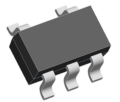
Space saving SOT23-5L package
Extended temperature range: -40°C to +125°C
The TF0215/16 high speed, low side MOSFET and IGBT
drivers are capable of driving 1.9A of peak current. The
TF0215/16 logic inputs are compatible with standard TTL
and CMOS levels (down to 3.3V) to interface easily with
MCUs. Internal undervoltage lockout (UVLO) will protect
MOSFET with loss of supply by turning off the output when
VCC falls below operating range. Fast and well matched
propagation delays allow high speed operation, enabling
a smaller, more compact power switching design using
smaller associated components.
These devices are highly resistant to noise by being able to
withstand up to 5V positive or negative on the ground pin
without damage. Also they can accept 500mA of reverse
current forced back into its outputs without damage or
logic change. The TF0215 provides an inverted output and
the TF0216 provides a noninverting output. The TF0215/16
comes in a space-saving SOT23-5L package and it operates
over an extended -40 °C to +125 °C temperature range.
Applications
Switch mode power supplies
Motor Drive
Line Drivers
DC-DC Converters
Ordering Information
Year Year Week Week
PART NUMBER PACKAGE
TF0215-USQ
SOT-23-5L
PACK / Qty
MARK
T&R / 3,000
TF0216-USQ
T&R / 3,000
T0215/16
YYWW
SOT-23-5L
SOT-23-5L
Typical Application
TO
LOAD
HINTF0215/16
OUT*/
VCC
OUT
LIN
VCC
IN/
IN*
www.tfsemi.com
Dec. 2020
R4
IN/IN*
COM
Rev. 1.2
1
�Advance Info
TF0215/16
High Speed, Low-Side, Single Gate Driver
Pin Diagrams
IN*
1
COM
2
IN
3
5
4
VCC
OUT*
TF0215
Pin Descriptions
PIN NAME
PIN NUMBER
IN*
Top View: SOT23-5L
1
COM
2
IN
3
5
VCC
4
OUT
TF0216
PIN DESCRIPTION
IN*
1
Logic input, in phase with OUT* (TF0215), out of phase with OUT (TF0216), leave open
when not in use.
COM
2
Supply return
IN
3
Logic input, out of phase with OUT* (TF0215), in phase with OUT (TF0216), leave open
when not in use.
OUT*/OUT
4
Gate drive output
VCC
5
Supply input
Functional Block Diagram
Dec. 2020
2
�Advance Info
TF0215/16
High Speed, Low-Side, Single Gate Driver
Absolute Maximum Ratings (NOTE1)
VCC - Low-side fixed supply voltage...............................-0.3V to +22V
VOUT - Output voltage (OUT/OUT*)........................-0.3V to VCC +0.3V
VIN - Logic input voltage (IN)....................................-5V to VCC +0.3V
ESD Protection on all pins....................................................2kV (HBM)
400V (MM)
NOTE1 Stresses beyond those listed under “Absolute Maximum Ratings” may cause
permanent damage to the device. These are stress ratings only, and functional operation
of the device at these or any other conditions beyond those indicated in the operational
sections of the specifications is not implied. Exposure to absolute maximum rating
conditions for extended periods may affect device reliability.
A
PD - Package power dissipation at TA ≤ 25 °C
SOT23-5L..........................................................................................TBD
SOT23-5L Thermal Resistance (NOTE2)
qJA ................................................................................................TBD °C/W
qJC................................................................................................TBD °C/W
TJ - Junction operating temperature........................................+150 °C
TL - Lead Temperature (soldering, 10 seconds).......................+300 °C
Tstg - Storage temerature ......................................................-55 to 150 °C
NOTE2 When mounted on a standard JEDEC 2-layer FR-4 board.
Recommended Operating Conditions
Symbol
Parameter
MIN
MAX
Unit
VCC
Supply voltage
4.5
18
V
VOUT
Output voltage (OUT/OUT*)
0
VCC
V
VIN
Logic input voltage (IN)
0
5
V
TA
Ambient temperature
-40
125
°C
Dec. 2020
3
�Advance Info
TF0215/16
High Speed, Low-Side, Single Gate Driver
Electrical Characteristics (NOTE3)
VBIAS (4.5V
很抱歉,暂时无法提供与“TF0216-USQ”相匹配的价格&库存,您可以联系我们找货
免费人工找货- 国内价格
- 1+1.96000
- 30+1.89000
- 100+1.75000
- 500+1.61000
- 1000+1.54000
- 国内价格
- 5+2.51100
- 50+1.96690
- 150+1.73362
- 500+1.44267