物料型号:TF2103M
器件简介:TF2103M是一款高电压、高速门驱动器,适用于驱动N沟道MOSFET和IGBT,特别适用于半桥配置。它采用TF Semiconductors的高电压工艺,能够在自举操作中将高侧切换至600V。
引脚分配:
- Vcc:逻辑和低侧电源
- HIN:高侧门驱动器输出的逻辑输入,与HO同相
- LIN:低侧门驱动器输出的逻辑输入,与LO反相
- COM:低侧和逻辑返回
- LO:低侧门驱动输出
- VS:高侧浮动电源返回
- HO:高侧门驱动输出
参数特性:
- 内部死区时间:420ns(典型值)
- 低侧门驱动电源电压:10V至20V
- 逻辑输入电压(HIN和LIN):3.3V能力,施密特触发逻辑输入
- 欠压锁定:VCC(逻辑和低侧电源)
功能详解:
- TF2103M设计用于在嘈杂的电机应用中提高性能,具有290mA源/600mA汇输出电流能力。
- 输出能够容忍负瞬变。
- 固定内部死区时间保护MOSFET。
应用信息:
- 电机控制
- DC-DC转换器
- AC-DC逆变器
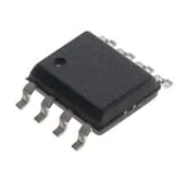
封装信息:
- SOIC-8(N)
- PDIP-8