Preliminary Datasheet
LP3993
200mA,Ultra-low Noise LDO Regulator
General Description
Features
The LP3993 is designed for portable applications with
Ultra-Low-Noise for RF Application
demanding performance and space requirements. The
Input Voltage up to 24V
Low Dropout : 300mV @ 100mA
Output Current 200mA
Ultra-Fast Response in Line/Load Transient
Current Limiting and Thermal Shutdown
LP3993 performance is optimized for high voltage
systems to deliver ultra low noise and low quiescent
current. Regulator ground current increases only
slightly in dropout, further prolonging the input system
life. The LP3993 also works with low-ESR ceramic
Protection
capacitors, reducing the amount of board space
necessary for power applications, critical in hand-held
wireless devices. The other features include ultra low
Applications
dropout voltage, high output accuracy, current limiting
PMP/PDA/MP3 players
protection, and high ripple rejection ratio.
Cellular and Mobile phone
RF Module
Sensor Module
Order Information
LP3993
□ □
□ □ □
F: Pb-Free
Package Type
B3: SOT23-3
Typical Application Circuit
VIN
Vout
OUT
VIN
X3: SOT89-3
GND
Output Type
10uF
10uF
33: 3.3V
36: 3.6V
50: 5.0V
LP3993-00
Apr.-2017
Email: marketing@lowpowersemi.com
www.lowpowersemi.com
Page 1 of 7
�Preliminary Datasheet
LP3993
Functional Pin Description
Package Type
Pin Configurations
SOT-23-3 / SOT89-3
3
4
SOT23-3
SOT89-3
TOP VIEW
TOP VIEW
2
1
1
2
3
Pin Description
Pin
SOT23-3
SOT89-3
1
1
3
2/4
2
3
Name
Description
GND
Ground.
Vin
Power Input Pin
Vout
Output Pin.
Marking Information
Device
Marking
LPS
LP3993-33B3F
2EYWX
Package
Shipping
SOT23-3
3K/REEL
SOT89-3
1K/REEL
SOT23-3
3K/REEL
SOT89-3
1K/REEL
SOT23-3
3K/REEL
SOT89-3
1K/REEL
LPS
LP3993-33X3F
3993
33YWX
LPS
LP3993-36B3F
2LYWX
LPS
LP3993-36X3F
36YWX
LPS
LP3993-50B3F
2KYWX
LPS
LP3993-50X3F
3993
50YWX
Marking indication:
Y:Production year W:Production week X: Series Number
LP3993-00
Apr.-2017
Email: marketing@lowpowersemi.com
www.lowpowersemi.com
Page 2 of 7
�Preliminary Datasheet
LP3993
Function Diagram
Absolute Maximum Ratings
Supply Input Voltage ------------------------------------------------------------------------------------------- -0.3V to 30V
Other pin to GND -------------------------------------------------------------------------------------------------- -0.3V to 8V
Maximum Junction Temperature ------------------------------------------------------------------------------------ 150°C
Maximum Soldering Temperature (at leads, 10 sec) ---------------------------------------------------------- 260°C
Operating Junction Temperature Range (T J) ---------------------------------------------------------- -40℃ to 85°C
Storage Temperature --------------------------------------------------------------------------------------- -65℃ to 165°C
Power Dissipation, PD @ TA = 25°C
SOT23-3 ----------------------------------------------------------------------------------------------------------------- 450mW
SOT89-3 ----------------------------------------------------------------------------------------------------------------- 700mW
Package Thermal Resistance
SOT23-3, θJA --------------------------------------------------------------------------------------------------------- 250°C/W
SOT89-3, θJA --------------------------------------------------------------------------------------------------------- 165°C/W
ESD Susceptibility
HBM (Human Body Mode) ------------------------------------------------------------------------------------------------ 2kV
MM(Machine-Mode) ------------------------------------------------------------------------------------------------------ 200V
LP3993-00
Apr.-2017
Email: marketing@lowpowersemi.com
www.lowpowersemi.com
Page 3 of 7
�Preliminary Datasheet
LP3993
Recommended Operating Conditions
Supply Input Voltage -------------------------------------------------------------------------------------- Vout+1V to 24V
Electrical Characteristics
(CIN = 10µF, COUT =10uF,Vin=Vout+1V,TA = 25°C, unless otherwise specified)
Parameter
Symbol
Test Conditions
Min
Typ.
Max
Units
Output Voltage Accuracy
ΔVOUT
IOUT = 1mA
−2
--
+2
%
Output Loading Current
Iout
Current Limit
ILIM
RLOAD = 1Ω
Quiescent Current
IQ
IOUT = 0mA
5
μA
Dropout Voltage
VDROP
IOUT = 100mA, VOUT =3.3V
300
mV
Linear Regulation
ΔVLINE
Load Regulation
ΔVLOAD
\Thermal Shutdown Temperature
TSD
200
VIN = (VOUT + 1V) to 12V,
IOUT = 1mA
1mA < IOUT < 150mA
Thermal Shutdown Hysteresis
LP3993-00
Apr.-2017
Email: marketing@lowpowersemi.com
mA
250
0.2
%
2
%
150
°C
25
°C
www.lowpowersemi.com
Page 4 of 7
�Preliminary Datasheet
LP3993
Applications Information
Like any low-dropout regulator, the external capacitors
The power dissipation definition in device is:
used with the LP3993 must be carefully selected for
regulator stability and performance. Using a capacitor
PD = (VIN−VOUT) x IOUT + VIN x IQ
whose value is ≥ 10µF on the LP3993 input. The
The maximum power dissipation depends on the
input capacitor must be located a distance of not more
thermal resistance of IC package, PCB layout, the rate
than 0.5 inch from the input pin of the IC and returned
of surroundings airflow and temperature difference
to a clean analog ground. Any good quality ceramic or
between junction and ambient.
tantalum can be used for this capacitor. The capacitor
The maximum power dissipation can be calculated by
with larger value and lower ESR (equivalent series
following formula:
resistance) provides better PSRR and line-transient
response. The output capacitor must meet both
PD(MAX) = ( TJ(MAX) − TA ) /θJA
requirements for minimum amount of capacitance and
Where TJ(MAX) is the maximum operation junction
ESR in all LDO`s application. The LP3993 is designed
temperature 125°C, TA is the ambient temperature and
specifically to work with low ESR ceramic output
the θJA is the junction to ambient thermal resistance.
capacitor
For recommended operating conditions specification
in
space-saving
and
performance
consideration. Using a ceramic capacitor whose value
is at least 10µF with ESR is > 25mΩ on the LP3993
output ensures stability. The LP3993 still works well
of LP3993, the junction to ambient thermal resistance
(θJA is layout dependent) for LP3993 showed below.
SOT23-3 : 250℃/W
with output capacitor of other types due to the wide
stable
ESR range.
Output
capacitor of
larger
capacitance can reduce noise and improve load
SOT89-3 : 165℃/W
And,
transient response, stability, and PSRR. The output
PD=(125°C−25°C)/250℃/W= 400mW (SOT23-3)
capacitor should be located not more than 0.5 inch
PD=(125°C−25°C)/165℃/W= 600mW (SOT89-3)
from the VOUT pin of the LP3993 and returned to a
The
maximum
power
dissipation
depends
on
clean analog ground.
operating ambient temperature for fixed T J(MAX) and
thermal resistance θJA.
Thermal Considerations
Thermal protection limits power dissipation in LP3993.
When the operation junction temperature exceeds
150°C, the OTP circuit starts the thermal shutdown
function turn the pass element off. The pass element
turns on again after the junction temperature cools by
25°C.
LP3993-00
Apr.-2017
Email: marketing@lowpowersemi.com
www.lowpowersemi.com
Page 5 of 7
�Preliminary Datasheet
LP3993
Packaging Information
SOT-89
LP3993-00
Apr.-2017
Email: marketing@lowpowersemi.com
www.lowpowersemi.com
Page 6 of 7
�Preliminary Datasheet
LP3993
SOT23-3
LP3993-00
Apr.-2017
Email: marketing@lowpowersemi.com
www.lowpowersemi.com
Page 7 of 7
�
很抱歉,暂时无法提供与“LP3993-33B3F”相匹配的价格&库存,您可以联系我们找货
免费人工找货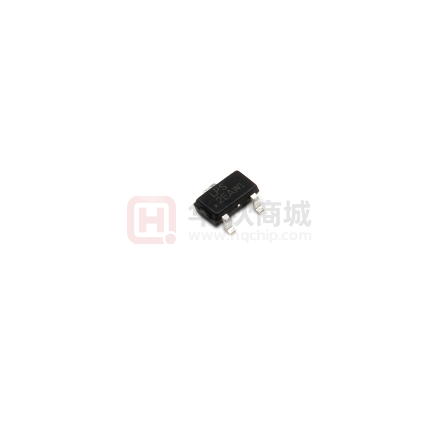


 工商网监
湘ICP备2023018690号
工商网监
湘ICP备2023018690号

