DATA SHEET
CURRENT SENSOR - LOW TCR
AUTOMOTIVE GRADE
PA1206_L series
5%, 1%
Product specification– July 24, 2017 V.2
RoHS compliant & Halogen free
�-
Product specification
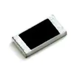
Chip Resistor Surface Mount
2
10
SERIES
PA1206_L
SCOPE
ORDERING INFORMATION - GLOBAL PART NUMBER
This specification describes PA
series current sensor - low TCR
with lead-free terminations made by
metal substrate.
Global part numbers are identified by the series, size, tolerance, packing
type, temperature coefficient, taping reel and resistance value.
GLOBAL PART NUMBER
PA XXXX X X X XX XXXX L
(1)
APPLICATIONS
Consumer goods
Computer
Telecom / Datacom
Industrial / Power supply
Alternative Energy
Car electronics
FEATURES
AEC-Q200 qualified
Halogen-free Epoxy
RoHS compliant
Reduce environmentally
hazardous wastes
(2) (3) (4)
(5)
(6)
(7)
(1) SIZE
1206
(2) TOLERANCE
D =± 0.5% (for 5mΩ and up)
F = ± 1%
J = ± 5%
(3) PACKAGING TYPE
R = Paper taping reel
(4) TEMPERATURE COEFFICIENT OF RESISTANCE
F = ± 100ppm/°C
M = ± 75ppm/°C
E= ± 50ppm/°C
(5) TAPING REEL
High component and
equipment reliability
07 = 7 inch dia. Reel & standard power (1/4W)
Non-forbidden materials used
in products/production
47 = 7 inch dia. Reel & 4 x standard power (1W)
Low resistances applied to
current sensing
7W = 7 inch dia. Reel & 2 x standard power (1/2W)
67 = 7 inch dia. Reel & 6 x standard power (1.5W)
(6) RESISTANCE VALUE
1 mΩ to 50 mΩ
(7) DEFAULT CODE
Letter L is the system default code for ordering only. (Note)
Resistance rule of global part
number
Resistance code rule
Example
0RXXX
(1 to 50mΩ)
0R001 = 1 mΩ
0R015 = 15 mΩ
ORDERING EXAMPLE
The ordering code of a PA1206 1/4W
chip resistor, TC100, value 0.003Ω with
±1% tolerance, supplied in 7-inch tape
reel is : PA1206FRF070R003L
NOTE
1. All our RChip products are RoHS compliant. "LFP" of the internal 2D reel label mentions
"Lead-Free Process"
www.yageo.com
Jul. 24, 2017 V.2
�-
Product specification
Chip Resistor Surface Mount
PA1206_L
3
10
SERIES
MARKING
PA1206
4 digits
The “R” is used as a decimal point; the other 3 digits are significant
PA1206: 1mΩ
Fig. 1
Fig. 2
Value = 1 mΩ
Value = 5 mΩ
4 digits
The “R” is used as a decimal point; the other 3 digits are significant
PA1206: 2mΩ to 50mΩ
CONSTRUCTION
The resistors are constructed using outstanding TCR level material, which makes Yageo P A resistors excellent
for current sensing application in battery charger circuit & DC -DC converter.
The composition of the resistive material is adjusted to give the approximate required resistance and is
covered with a protective coating. Marking is printe d on the top side of the resistor.
Finally, the three external terminations (Cu / Ni / matte Tin) are added, as shown in Fig. 3.
Outlines
For dimensions, please refer to Table 1
Fig. 3 Chip resistor outlines
www.yageo.com
Jul. 24, 2017 V.2
�-
Product specification
Chip Resistor Surface Mount
PA1206_L
4
10
SERIES
DIMENSION
Table 1 For outlines, please refer to Fig. 3
TYPE
RESISTANCE RANGE POWER RATING
L (mm)
W (mm)
H (mm)
I1 (mm)
I2 (mm)
1/4W
1/2W
1W
1.5W (1~5mΩ)
3.20 ± 0.25
1.60±0.25
0.65±0.25
1.04±0.25
1.04±0.25
3.20 ± 0.25
1.60±0.25
0.65±0.25
0.64±0.25
0.64±0.25
3.20 ± 0.25
1.60±0.25
0.65±0.25
0.51±0.25
0.51±0.25
1mΩ
PA1206
2mΩ ≤ R ≤ 5mΩ
6mΩ ≤ R ≤ 50mΩ
Note:
1. For relevant physical dimensions, please refer to construction outlines.
2. Please contact with sales offices, distributors and representatives in your region before ordering.
ELECTRICAL CHARACTERISTICS
Table 2
SERIES
SIZE
POWER RATING
TOLERANCE
1/4W
1/2W
Fig. 4
PA
Chip resistor outlines
1W
1206
± 1%
± 5%
1.5W
RESISTANCE RANGE
TEMPERATURE COEFFICIENT
OF RESISTANCE
1mΩ ≤ R ≤ 2mΩ
± 75ppm/°C, ± 100ppm/°C
3mΩ ≤ R ≤ 50mΩ
± 50ppm/°C, ± 75ppm/°C, ± 100ppm/°C
1mΩ ≤ R ≤ 2mΩ
± 75ppm/°C, ± 100ppm/°C
3mΩ ≤ R ≤ 5mΩ
± 50ppm/°C, ± 75ppm/°C, ± 100ppm/°C
Note: Please contact with sales offices, distributors and representatives in your region before ordering.
FUNCTIONAL DESCRIPTION
OPERATING TEMPERATURE RANGE
PA1206 Range: –55°C to +170°C
POWER RATING
Standard rated power at 70°C:
For detail power value, please refer to Table 2.
RATED VOLTAGE
The DC or AC (rms) continuous working voltage
corresponding to the rated power is determined by
the following formula:
V = (PxR )
Where
Fig. 4 Maximum dissipation (Pmax ) in percentage of rated power
as a function of the operating ambient temperature (T amb)
V = Continuous rated DC or
AC (rms) working voltage (V)
P = Rated power (W)
R = Resistance value (Ω)
www.yageo.com
Jul. 24, 2017 V.2
�-
Product specification
Chip Resistor Surface Mount
PA1206_L
5
10
SERIES
PACKING STYLE AND PACKAGING QUANTITY
Table 3 Packing style and packaging quantity
PACKING STYLE
REEL DIMENSION
PA1206
7" (178 mm)
4,000
Paper Taping Reel (R)
EMBOSSED TAPE
Fig. 5 Embossed Tape
Table 4 Dimensions of embossed tape for relevant chip resistors size
SIZE
SYMBOL
A0
Unit: mm
B0
PA1206 1.90± 0.10 3.50± 0.10
W
E
F
P0
P1
P2
Ø D0
Ø D1
T
8.00± 0.30
1.75± 0.10
3.50± 0.10
4.00± 0.10
4.00± 0.10
2.00± 0.10
1.55± 0.05
1.50± 0.10
1.50± 0.10
www.yageo.com
Jul. 24, 2017 V.2
�-
Product specification
Chip Resistor Surface Mount
PA1206_L
6
10
SERIES
REEL SPECIFICATION
Fig. 6 Reel
HBK039
Table 5 Dimensions of reel specification for relevant chip resistors size
QUANTITY
PER REEL
SIZE
PA1206
REEL SIZE
8 mm
TAPE WIDE
12 mm
TAPE WIDE
--
7"
(Ø 178 mm)
4000
SYMBOL
A
180.0+0/-3
Unit: mm
N
60.0+1/-0
C
13.0± 0.2
D
21.0± 0.8
W1
W2 MAX.
8.4 +1/-0
12.4
LEADER/TRAILER TAPE SPECIFICATION
Fig. 7 Leader/Trailer Tape
CCB325
www.yageo.com
Jul. 24, 2017 V.2
�-
Product specification
Chip Resistor Surface Mount
PA1206_L
7
10
SERIES
FOOTPRINT AND SOLDERING PROFILES
For recommended soldering profiles, please refer to data sheet “Chip resistors mounting”.
FOOTPRINT
Fig. 8 Single resistor chips recommended dimensions of footprints
Table 6 Footprint dimensions
Unit: mm
SIZE
RESISTANCE RANGE
PA1206
1mΩ ≤ R ≤ 50mΩ
A
B
C
D
3.90
0.76
1.57
1.78
www.yageo.com
Jul. 24, 2017 V.2
�-
Product specification
Chip Resistor Surface Mount
PA1206_L
8
10
SERIES
TESTS AND REQUIREMENTS
Table 7 Test condition, procedure and requirements
TEST
TEST METHOD
Short time
overload
IEC60115-1 4.13
High Temperature
Exposure
MIL-STD-202-Method 108
PROCEDURE
REQUIREMENT
5 times of rated power for 5 seconds at
room temperature
± (0.5%+0.0005Ω)
1,000 hours at maximum operating
temperature depending on specification,
unpowered
± (1.0%+0.0005Ω)
No visible damage
No direct impingement of forced air to
the parts Tolerances: 170± 3ºC
Temperature
Cycling
JESD22-A104C
1,000 cycles, -55/+125ºC for 1 cycle per
hour
± (0.5%+0.0005Ω)
Moisture
Resistance
MIL-STD-202-Method 106
Each temperature / humidity cycle is
defined at 8 hours (method 106F), 3
cycles / 24 hours for 10d with 25ºC /
65ºC 95% R.H, without steps 7a & 7b,
unpowered
± (0.5%+0.0005Ω)
Biased
Humidity
MIL-STD-202 Method 103
1,000 hours; 85ºC / 85% RH
± (0.5%+0.0005Ω)
Operational Life/
Endurance
MIL-STD-202-Method 108
10% of operating power
1,000 hours at 125± 3ºC, de-rated voltage
applied for 1.5 hours on, 0.5 hour off, stillair required
± (1.0%+0.0005Ω)
1,000 hours at 70± 2ºC applied RCWV
± (1.0%+0.0005Ω)
1.5 hours on, 0.5 hour off, still air required
Resistance to
Solvents
MIL-STD-202 Method 215
Immerse in isopropyl alcohol for 5 min
with ultrasonic at room temperature
No Visible damage
Mechanical Shock
MIL-STD-202 Method 213
Three shocks in each direction shall be
applied along the three mutually
perpendicular axes of the test specimen.
± (0.5%+0.0005Ω)
Peak value: 100 g’s
Duration: 6 ms
Velocity change: 12.3 ft/s
Waveform: Half sine
Vibration
MIL-STD-202 Method 204
5 g’s for 20 min., 12 cycles each of 3
orientations
± (0.5%+0.0005Ω)
Test from 10-2000 Hz.
Resistance to
Soldering Heat
MIL-STD-202-method 210
Condition B, no pre-heat of samples
± (0.5%+0.0005Ω)
Leadfree solder, 260ºC, 10 seconds
immersion time
No visible damage
Procedure 2 for SMD: devices fluxed and
cleaned with isopropanol
Thermal Shock
MIL-STD-202 Method 107
-55/+125ºC, Number of cycles is 300.
Devices mounted.
± (0.5%+0.0005Ω)
No visible damage
Maximum transfer time is 20 seconds.
Dwell time is 15 minutes. Air -Air
www.yageo.com
Jul. 24, 2017 V.2
�-
Product specification
Chip Resistor Surface Mount
TEST
TEST METHOD
Electrostatic
Discharge
AEC-Q200-002
Solderability
- Wetting
J-STD-002B test B
PA1206_L
PROCEDURE
9
10
SERIES
REQUIREMENT
Human Body Model, 1 pos + 1 neg.
± (1.0%+0.0005Ω)
Discharges 1206=2KV
No visible damage
(a) Method B, aging 4 hours at 155ºC dry
heat, dipping at 235± 3ºC for 5± 0.5
seconds.
Well tinned
(>95% covered)
No visible damage
(b) Method B, steam aging 8 hours,
dipping at 215± 3ºC for 5± 0.5
seconds.
(c) Method D, steam aging 8 hours,
dipping at 260± 3 ºC for 7± 0.5
seconds.
Flammability
UL94
Try to inflame a specimen by a needle
flame
No ignition of specimen;
V-0
Board Flex /
Bending
AEC-Q200-005
Chips mounted on a 90mm glass epoxy
resin PCB (FR4), Bending for 1206=2 mm
± (1.0%+0.0005Ω)
Holding time: Min.60 seconds
Terminal
Strength (SMD)
AEC-Q200-006
Flame Retardance
Temperature
Coefficient of
Resistance (T.C.R.)
Applied a 17.7N (1.8Kg) for 60± 1
seconds.
± (1.0%+0.0005Ω)
AEC-Q200-001
Apply voltage from 9V to 32V to increase
the surface temp to 350ºC
No flame,
no explosion
MIL-STD-202 Method 304
At +25/+150ºC
Refer to table 2
No visible damage
Formula:
T.C.R=
R 2 R1
x106(ppm/ºC)
R1( t 2 t1)
Where
t1=+25ºC or specified room temperature
t2=+150ºC test temperature
R1=resistance at reference temperature in
ohms
R2=resistance at test temperature in ohms
Flower-of-Sulfur
(FOS)
Modified ASTM B809-95
Sulfur 105ºC, 750 hours, unpowered.
± (1.0%+0.0005Ω)
www.yageo.com
Jul. 24, 2017 V.2
�-
Product specification
Chip Resistor Surface Mount
PA1206_L
10
10
SERIES
REVISION HISTORY
REVISION
DATE
Version 2TYPE Jul. 24, 2017
CHANGE NOTIFICATION
-
POWER
DESCRIPTION
TEMPERATURE COEFFICIENT
RESISTANCE
RANGE
TOLERANCE
- Add part number
coding details
for the relationship between
taping reel
OF RESISTANCE
3/10W, 2/5W, 1/2W
0603 1/10W, 1/5W,
May 05, 2017 1/8W, 1/4W, 1/3W, 1/2W
0805
1/4W, 1/2W
Version 01206
Mar. 31, 2017 Version 1
and rated power
5 mΩ ≦ R < 100 mΩ
- Extend resistor value
4 mΩ ≦ R < 100 mΩ
mΩ
≦ R < 100
mΩ current sensor –PA1206_L series.
- New datasheet 3for
automotive
grade
1/2W, 1W
PF
The resistors are constructed
using outstanding TCR level
material, which makes Yageo PF
resistors excellent for current
sensing application in battery
charger circuit & DC-DC
converter.
The composition of the resistive
2010 material is adjusted to give the
approximate required resistance
and is covered with a protective
coating, which printed with the
resistance value.
Finally, the three external
terminations (Ni / matte Tin) are
added, as shown in Fig. 4.
2512
4527
± 1%
± 2%
5 mΩ ≦ R < 100 mΩ
±75 ppm/°C
± 5%
1W, 2W
1 mΩ ≦ R < 100 mΩ
3W
1 mΩ ≦ R ≦ 50 mΩ
2W, 3W, 5W
6 mΩ ≦ R < 1Ω
NOTE: 1. PLEASE CONTACT WITH SALES OFFICES, DISTRIBUTORS AND REPRESENTATIVES IN YOUR REGION BEFORE ORDERING
“ Yageo reserves all the rights for revising the content of this datasheet without further notification, as long as the products itself are unchanged. Any
product change will be announced by PCN.”
www.yageo.com
Jul. 24, 2017 V.2
�