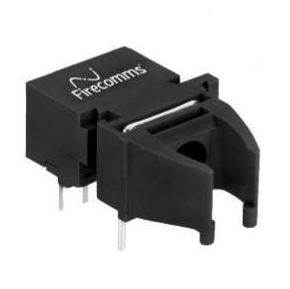
FR50MxxR
DC-50 MBd RedLink® Fibre Optic Receiver
Datasheet
DESCRIPTION
The Firecomms DC-50 MBd RedLink® receiver is a
fully integrated photodiode and receiver IC. The
receiver is housed in a miniature package to
interface to plug-terminated lengths of Plastic Optic
Fiber (POF) or 200 μm Plastic Clad Silica (PCS) fiber.
When paired with the appropriate transmitter, the
receiver is capable of delivering 50 Mbps digital
signals over fiber and operate in the temperature
range of -40 ⁰C to +85 ⁰C. The device can operate
from 5V or 3.3V DC power rails and can tolerate +/10% supply variation.
The receiver is a robust optical to electrical receiver
with integrated pulse width distortion minimization
circuitry for reliable data transmission. The receiver
features a push-pull TTL compatible CMOS output.
It is available in inverting and non-inverting options.
AVAILABLE OPTIONS
Table 1
ORDERING INFORMATION / PART NUMBERS
50 MBd Horizontal Package
Non-Inverting
FR50MHNR
50 MBd Horizontal Package
Inverting
FR50MHIR
50 MBd Vertical Package
Non-Inverting
FR50MVNR
50 MBd Vertical Package
Inverting
FR50MVIR
50 MBd 30⁰ Tilted Package
Non-Inverting
FR50MWNR
50 MBd 30⁰ Tilted Package
Inverting
FR50MWIR
FEATURES
•
Ideal for use with POF or PCS fiber
•
Optimized for data transmission from DC-50
MBd
•
Industrial Temperature Range -40 ⁰C to +85 ⁰C
•
Dual 5 V and 3.3 V power supply with 10 % rail
tolerance
•
RoHS compliant and flame retardant
(UL 94 V-0)
•
Inverting and Non-Inverting options available
•
Horizontal Vertical and 30⁰ Tilted options
available
•
Push Pull TTL Compatible CMOS output
•
Ultra-low pulse width distortion to limit pulse
distortion from burst mode data
•
Compatible with Versatile Link cables and
connectors
APPLICATIONS
Table 2
APPLICATIONS
Application
Automation and Industrial Control. Serial
Communications. Voltage Isolation.
Standard
Serial RS232, RS485, CAN-Bus, MODBUS,
Profibus
Distance
50 meters Step Index POF [1]
300 meters with 200 µm PCS fiber [1]
Speed
DC to 50 MBd
Note: 1. Depending on the installation conditions
FR50MxxR Revision F
1
�SPECIFICATIONS
5, Gnd
Table 3
RECEIVER PIN DESCRIPTION
4, N.C.
Pin
Name
Symbol
3, Vcc
1
Receiver Output
V0
2
Receiver Ground
GND
2, Gnd
3
Receiver Vcc
Vcc
1, VO
4
No Connect (a)
N.C.
5
Retaining Pin (b)
GND
8
Retaining Pin (b)
GND
NOTE:
a)
b)
IC
8, Gnd
FIGURE 1 Receiver pin-out, top view
Pin 4 is electrically isolated internally. Pin 4 may be externally connected to pin 1 for board layout compatibility with existing
designs. Otherwise it is recommended pin 4 be grounded as in Figure 2
Pins 5 and 8 are used for mounting and retaining purposes. Connect to ground
RECOMMENDED APPLICATION CIRCUIT
5
1 µH
4
3
IC
100 nF
10 µF
Vcc
10 µF
2
1
8
Data TTL Output
FIGURE 2 RedLink® Receiver Application Circuit
FR50MxxR Revision F
2
�GENERAL OPERATION FOR INVERTING RECEIVER
50%
Optical Input, Pin
tPropDly-HL
tPropDly-LH
90%
50%
10%
Receiver Output, Vo
tf
tr
FIGURE 3
Receiver Propagation Delay and rise/fall time definitions for an inverting receiver output
Data Input
(Optical)
Vcc
~2.8V
~2.6V
40 µs
Data Output
Vo
Vo = High Impedance
Vo = High Impedance
FIGURE 4
Inverting receiver output operation during power cycling
Operation of the Inverting parts FR50MxIR during power up, power down or power reset is
illustrated above. During power up as Vcc rises to approximately 2.8 V, the output Vo is in a
high impedance state. Within 40 µs of Vcc reaching 2.8 V the output Vo will change to the
correct logic state which in the diagram above is logic low as there is light present and the
output is inverted relative to the light input. On power down once Vcc drops below
approximately 2.6 V then Vo changes immediately to a high impedance state.
FR50MxxR Revision F
3
�GENERAL OPERATION FOR NON-INVERTING RECEIVER
50%
Optical Input, Pin
tPropDly-LH
tPropDly-HL
90%
50%
10%
Receiver Output, Vo
tr
tf
FIGURE 5
Receiver Propagation Delay and rise/fall time definitions for a non-inverting receiver output
Data Input
(Optical)
Vcc
~2.8V
~2.6V
40 µs
Data Output
Vo
Vo = High Impedance
Vo = High Impedance
FIGURE 6
Non-Inverting receiver output operation during power cycling
Operation of the Non-Inverting parts FR50MxNR during power up, power down or power
reset is illustrated above. During power up as Vcc rises to approximately 2.8 V, the output Vo
is in a high impedance state. Within 40 µs of Vcc reaching 2.8 V the output Vo will change to
the correct logic state which in the diagram above is logic high as there is light present and
the output is non-inverting. On power down once Vcc drops below approximately 2.6 V then
Vo changes immediately to a high impedance state.
FR50MxxR Revision F
4
�SPECIFICATIONS
Table 4
REGULATORY COMPLIANCE
Parameter
Symbol
Standard
Level
Electrostatic Discharge,
Human Body Model (contact ESD)
HBM
Mil-STD-883
Level 2 (4 kV)
Radiated Emissions Immunity
Vm-1
IEC 61000-4-3
15 Vm-1
60950-1
File No. E362227
UL Certification
UL
Storage Compliance
MSL
J-STD-020
2a (4 week floor life)
Restriction of Hazardous
Substances Directive
RoHS
Directive 2011/65/EU
Certified compliant
Table 5
ABSOLUTE MAXIMUM RATINGS
These are the absolute maximum ratings at or beyond which the FOT can be expected to be damaged
Notes:
1. 260°C for 10 seconds, one time only, at least 2.2 mm away from lead root
Parameter
Symbol
Minimum
Maximum
Unit
Storage Temperature
Tstg
-40
+85
°C
Operating Temperature
Top
-40
+85
°C
Soldering Temperature [1]
Tsld
+260
°C
Receiver Supply Voltage
Vcc
-0.5
+5.5
V
Receiver Output Current
IO
-16
+16
mA
FR50MxxR Revision F
5
�SPECIFICATIONS
Table 6
RECEIVER ELECTRICAL AND OPTICAL CHARACTERISTICS
Test Conditions:
1. Wake up Delay is the delay from VCC > 2.75 V to when the output will respond correctly to optical input. Output is held in
tristate before this time
2. Test data was validated using a transmitter with an emission wavelength between 635 and 680 nm, with a 5ns rise and fall
time, over the full temperature range of -40 °C to +85 °C, over both supply rail voltage options of 5 V and 3.3 V ± 10%, and
over the input optical received power as specified by PH and PL. Input power levels are for peak (not average) optical input
levels. For 50% duty cycle data, peak optical power is twice the average optical power. Data referred to as typical are rated
at +25 °C
3. Optical signal from the recommended Transmitter circuit.
4. Testing in the recommended receiver circuit (RL= 50 kΩ, CL(total)= 15 pF).
5. PWD for Optical Input of 50 MBd, NRZ 27-1 (PRBS7) data, resulting in a BER ≤ 10-9.
6. PWD for 1st to 3rd pulse is characterized with minimum Optical Input pulse width of 20 ns, with the 1st pulse being the
worst case. For pulses > 20 ns the PWD will be less. If data rate < 1 MBd, then the pulse width distortion = PWD 1st to 3rd
pulse.
7. The performance of the receiver as given in Table 6 has been characterized for transmitters operating between 635 and 680
nm. The receiver will nevertheless respond to optical sources operating from the visible to near infra-red regions although
the precise performance may differ from that given in Table 6 depending upon the precise wavelength and rise/fall time
characteristics of the optical source used.
Parameter
Supply Current
Wake Up Delay (power up)
Symbol
Min
Typical
Max
Unit
Test Condition
ICC
20
25
mA
[2,3,4]
tpower-on
40
µs
[1]
High Level Output Voltage
VOH
Vcc – 0.05
Vcc
V
IOH-max = 40 µA, [2]
Low Level Output Voltage
VOL
0
0.05
V
IOL-max=1.6 mA, [2]
Optical Power High (OPH)
PH
-22
+2
dBm
[2,3]
Optical Power Low (OPL)
PL
-40
dBm
[2,3]
50
MBd
Min UI = 20 ns
Max f = 25 MHz
Data Rate
DC
Output Rise Time (10% - 90%)
tr
5
ns
[2,3,4]
Output Fall Time (10% - 90%)
tf
5
ns
[2,3,4]
Pulse Width Distortion for PH range
-20 to + 2 dBm
PWD
-4
+4
ns
[2,3,4,5]
Pulse Width Distortion for PH range
-20 to -22 dBm
PWD
-6
+6
ns
[2,3,4,5]
PWDinit
-7
+14
ns
[2,3,4,5,6]
tPropDly-HL
50
ns
[2,3,4]
tPropDly-LH
50
ns
[2,3,4]
900
nm
[7]
Pulse Width Distortion
1st to 3rd pulse
Propagation Delay
Optical Sensitivity Range
λR
400
FR50MxxR Revision F
6
�0.64
3.56 min.
3.81 max.
4.2
7.62
MECHANICAL DATA, HORIZONTAL
2.54 (3x)
0.64 (2x)
0.25 (4X)
0.5 (4x)
7.62
Front View
Rear View
Side View
7.62
Dust Cap
2.54 (3x)
01
1.
Ø
1.27
x)
(6
Pin 1 Indicator
Date Code
2
2.83
1.27
1
7.62
8
1.90 min.
5
22.9
2
5.08
3
10.16
4
12.35
Product Number
18.9
PCB Hole Details
Top View
Top View
26.9
16.2
FIGURE 7
Mechanical dimensions of the horizontal receiver connectors and PCB footprint, which is a top view
General dimensional tolerance is ± 0.2 mm
Part Name: RedLink Xx
Lot No: TD20160402006
Part Number: XXXXXXXX
Date Code: 1622A
Quantity: 40
515
FIGURE 8
Packing tube for Firecomms Horizontal RedLink® Receivers
FR50MxxR Revision F
7
�MECHANICAL DATA, VERTICAL
Product Number
2.54 (3x)
0.5 (4x)
18.90
0.64
2.79 min.
3.30 max.
4.2
Date Code
0.25 (4X)
Ø0.64 (2x)
7.62
5.08
10.16
Pin 1 Indicator
Front View
Ø
1.
0
1
Rear View
Side View
4.42
2.0
Dust Cap
1.57
(6
x)
5
7.62
1.74
8
2
3
4
22.9
1
18.28
1.27
2.54 (3x)
Top View
7.62
PCB Hole Details
Top View
20.7
FIGURE 9
Mechanical dimensions of the vertical receiver connectors and PCB footprint, which is a top view
General dimensional tolerance is ± 0.2 mm
30.6
Part Name: RedLink Xx
Lot No: TD20160402006
Part Number: XXXXXXXX
Date Code: 1632E
Quantity: 40
515
FIGURE 10
Packing tube for Firecomms Vertical RedLink® Receivers
FR50MxxR Revision F
8
�Front View
0.56
4.40 min.
4.60 max.
2.54 (3x)
30°
10.4
15.24
MECHANICAL DATA, 30⁰ TILTED
0.25 (4x)
0.64 (4x)
0.5 (4x)
8.70
Rear View
Side View
7.62
1.27
2.54 (3x)
Pin 1 Indicator
3
2
1
8.70
4
2.20 min.
5
8
Dust Cap
2
01
1.
10.16
Ø
Date Code
x)
(6
5.08
6.82
1.27
Product Number
17.72
22.9
19.3
PCB Hole Details
Top View
Top View
21
FIGURE 11
Mechanical dimensions of the tilted receiver connectors and PCB footprint, which is a top view
General dimensional tolerance is ± 0.2 mm
27.1
Part Name: RedLink Xx
Lot No: RD20160402006
Part Number: XXXXXXXX
Date Code: 1632E
Quantity: 40
515
FIGURE 12
Packing tube for Firecomms Tilted RedLink® Receivers
FR50MxxR Revision F
9
�PART HANDLING
The Firecomms DC-50 RedLink® receiver devices are color coded black. They are auto-insertable. They
are tested for handling in static-controlled assembly processes (HBM). Cleaning, degreasing and post
solder washing should be carried out using standard solutions compatible with both plastics and the
environment. For example, recommended solutions for degreasing are alcohols (methyl, isopropyl and
isobutyl). Acetone, ethyl acetate, phenol or similar solution based products are not permitted.
In the soldering process, non-halogenated water soluble fluxes are recommended. These products are
not suitable for use in reflow solder processes (infrared/vapor-phase reflow). The dust plug should
remain in place during soldering, washing and drying processes to avoid contamination of the active
optical area of each part.
The Moisture Sensitivity Level (MSL) classification of this device is 2a according to JEDEC J-STD-020.
The shelf life of an unopened MBB (Moisture Barrier Bag) is 24 months at < 40 °C and < 90 % R.H.
Once the Moisture Barrier Bag is opened the devices can be either
a) Stored in normal factory conditions < 30 °C and < 60 % R.H. for a maximum of 672 hours
(4 Weeks) prior to soldering
b) Stored at < 10 % R.H. (Dry Cabinet)
FR50MxxR Revision F
10
�PACKING INFORMATION
Components are packed in PVC anti-static tubes in moisture barrier bags. Bags should be opened only
in static-controlled locations, and standard procedures should be followed for handling moisture
sensitive components.
Table 7
PACKING INFORMATION
Horizontal
Vertical
Tilted
40
40
40
Tube Length
515 mm
515 mm
515 mm
Tube Height
16.2 mm
21.0 mm
21 mm
Tube Depth
26.9 mm
30.8 mm
27.1 mm
Tubes per Bag
5
5
5
Bags per Inner Carton
1
1
1
Inner Carton Length
630 mm
630 mm
630 mm
Inner Carton Width
70 mm
70 mm
70 mm
Inner Carton Height
105 mm
105 mm
105 mm
0.77 kg
0.92 kg
0.92 kg
Components per Inner Carton
200
200
200
Inner Cartons per Outer Carton
10
10
10
Outer Carton Length
650 mm
650 mm
650 mm
Outer Carton Width
235 mm
235 mm
235 mm
Outer Carton Height
376 mm
376 mm
376 mm
8.15 kg
9.61 kg
9.60 kg
2,000
2,000
2,000
Components per Tube
Weight per Inner Carton,
Complete
Weight per Outer Carton,
Complete
Components per Outer Carton
For the most recent revision or further information please visit www.firecomms.com or contact the company directly at the
following address, Firecomms Ltd, 2200 Airport Business Park, Cork, IRELAND. Copyright© 2004-2019 Firecomms. All rights
reserved. Firecomms refers to Firecomms Limited and/or its subsidiaries. Firecomms assumes no responsibility for
inaccuracies or omissions in the information contained in this document. Specifications are subject to change without notice.
No patent rights are granted to any of the circuits described herein.
FR50MxxR Revision F
11
�