NS2009
4-Wire Touch Screen Controller with I2C Interface
NS2009 DataSheet V1.1
ShenZhen Nsiway Technology Co., Ltd
201108
1/19
�NS2009
4-Wire Touch Screen Controller with I2C Interface
Change History
DATA
2011,09
VERSION
V1.1
ShenZhen Nsiway Technology Co., Ltd
AUTHOR
CHAGE EXPLAIN
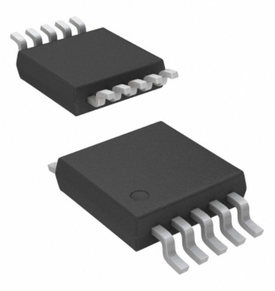
QFN(3×3)-16L
2/19
�NS2009
4-Wire Touch Screen Controller with I2C Interface
CONTENTS
Change History ..................................................................................................................................................................... 2
General Description ............................................................................................................................................................. 5
Features .................................................................................................................................................................................. 5
Applications........................................................................................................................................................................... 5
Typical Application Circuit................................................................................................................................................. 5
Absolute Maximum Ratings............................................................................................................................................... 6
Electrical Characteristics .................................................................................................................................................. 7
Pin Layout ............................................................................................................................................................................ 8
Pin Discription...................................................................................................................................................................... 9
Typical Characteristics ....................................................................................................................................................... 9
Theory of Operation......................................................................................................................................................... 11
The Basic Principle........................................................................................................................................................... 11
Analog Input Characteristics ........................................................................................................................................... 11
Differential Mode............................................................................................................................................................... 12
Application Recommendations of Touch Screen......................................................................................................... 12
Pressure Measurement.................................................................................................................................................... 12
Digital Interface................................................................................................................................................................... 13
Write Command ................................................................................................................................................................ 13
Read Command ................................................................................................................................................................ 14
High-Speed Mode............................................................................................................................................................. 14
Digital Timing..................................................................................................................................................................... 14
Data Format....................................................................................................................................................................... 16
PENIRQ Output................................................................................................................................................................. 16
Application Note ................................................................................................................................................................. 17
Physical Size of Chip Package ...................................................................................................................................... 18
MSOP-10 Package........................................................................................................................................................... 18
QFN(3×3)-16L Package................................................................................................................................................... 19
ShenZhen Nsiway Technology Co., Ltd
3/19
�NS2009
4-Wire Touch Screen Controller with I2C Interface
FIGURE LISTS
Figure1. NS2009 Typical Application Circuit .................................................................................................................. 5
Figure 2. MSOP-10 Package Pin Distribution (top view) ................................................................................................. 8
Figure 3. QFN(3×3)-16L Package Pin Distribution (top view)......................................................................................... 8
Figure 4. NS2009 Analog Input Schematic..................................................................................................................... 11
Figure 5. Differential reference mode diagram (C3 = 1, Y direction drive switch closure, XP as an analog input)....... 12
Figure 6. Pressure Measurement Block Diagram............................................................................................................ 12
Figure 7. I2C interface write command timing diagram ................................................................................................. 13
Figure 8. I2C Interface Read Command Timing Schamatic ........................................................................................... 14
Figure 9. NS2009 Digital Interface ................................................................................................................................. 14
Figure 10.Ideal Input Voltages and Output Codes .......................................................................................................... 16
Figure 11. PENIRQ Function Schematic ....................................................................................................................... 16
Figure 12. MSOP-10 Package Size ................................................................................................................................. 18
Figure 13.QFN(3×3)-16L Package Size.......................................................................................................................... 19
TABLE LISTS
Table 1 Chip Limit Parameter Table........................................................................................................................... 6
Table 2 NS2009 Electrical Characteristics Table ...................................................................................................... 7
Table 3 ADC Input Configuration ............................................................................................................................... 11
Table 4 address byte.................................................................................................................................................... 13
Table 5 Command Byte ............................................................................................................................................... 13
Table 6 PD0 Control Bit.............................................................................................................................................. 13
Table 7 timing specification......................................................................................................................................... 15
ShenZhen Nsiway Technology Co., Ltd
4/19
�NS2009
4-Wire Touch Screen Controller with I2C Interface
General Description
The NS2009 is a 4-wire resistive touch screen controller with I2C Interface, includes 12-bit resolution A / D converter.
The NS2009 through the implementation of the two A / D conversion has been identified by the location of the screen, in
addition to measurable increase in pressure on the touch screen. 2.7V typical work in the state, the closure of
the reference voltage, power consumption can be less than 0.75mW.
Features
Operating voltage range of 2.0V ~ 5.5V
Touch-pressure measurement
2-wire I2C communication interface
With automatic power down feature
MSOP10 and QFN(3×3)-16L package
-40 ~ 85 ℃ Operating Temperature Range
Applications
Mobile phone (cell phone, etc.)
Touch screen displays, personal digital assistant (PDA)
Portable equipment, POS terminal machine equipment, etc.
Typical Application Circuit
Figure1. NS2009 Typical Application Circuit
ShenZhen Nsiway Technology Co., Ltd
5/19
�NS2009
4-Wire Touch Screen Controller with I2C Interface
Absolute Maximum Ratings
Table 1 Chip Limit Parameter Table
Name
Parameter
VDD Voltage
-0.3V To +5.5V
Analog Input Voltage
-0.3V To +VDD+0.3V
Digital Input Voltage
-0.3V To+VDD+0.3V
Consumption
1W
Maximum Junction Temperature
+150℃
Operating Temperature
-40℃~+85℃
Storage Temperature
-65℃~+150℃
Welding Temperature (less than 10 seconds)
+260℃
ESD
+/- 8000V (HMD)
Latch Up
+/- 100mA
WARNING: In addition to limits or any other conditions, the chip may be damaged.
ShenZhen Nsiway Technology Co., Ltd
6/19
�NS2009
4-Wire Touch Screen Controller with I2C Interface
Electrical Characteristics
Qualification: VS = +2.5 V ~ +5.5 V, TA =- 40 ℃ ~ +85 ℃ , VDD = +2.7 V, 12 bits standard mode
(100K), or fast mode (400K), the digital input ground or VDD.
Table 2 NS2009 Electrical Characteristics Table
Parameter
Condition
Min
Typ
Max
Unit
Analog Input:
Differential Input
Cathode Input - Negative Input
Single-ended Input
0
VREF
V
Cathode Input
-0.2
+VDD+0.2
V
Negative Input
-0.2
+0.2
V
Input Capacitance
25
pF
Leakage current
0.1
µA
12
Bits
ADC System Performance:
Resolution
No missing Code
10
Bits
1
Integral Linearity Error
±2
LSB
Imbalance Error
±6
LSB
Gain Error
External Vref
Noise Performance
Including Internal Vref
±4
LSB
70
µVrms
70
dB
YP、XP
5
Ω
YN、XN
5
Ω
PSRR
Switch Driver
Switch On-Resistance
Driver Current(2)
Duration 100ms
50
mA
15
pF
Digital Input/Output
Logic Type
CMOS
Capacitance
All Digital Control Input Pins
VIH
| IIH |≤+5µA
VDD*0.7
VDD+0.3
V
VIL
| IIL |≤+5µA
-0.3
0.3*VDD
V
VOH
IOH=-250µA
VDD*0.8
VOL
IOL=250µA
Data Format
5
V
0.4
V
Straight
Binary
Power Requirement
VDD
Operating Range
Quiescent Current
Internal Vref Off
100
Internal Vref On
300
2.0
Power-Down State
5.5
V
150
µA
µA
3
µA
+85
℃
Temperature Range
Feature
-40
Notes:
1. LSB that the least significant bit
2. In order to ensure reliable chip, X, Y can not be larger than the drive current 50mA
ShenZhen Nsiway Technology Co., Ltd
7/19
�NS2009
4-Wire Touch Screen Controller with I2C Interface
Pin Configuration
Pin Layout
Figure 2. MSOP-10 Package Pin Distribution (top view)
16
15
14
13
QFN(3*3)-16 marking
1
12
NC
A0
2
11
BAT
GND
3
10
GND
A1
XD2009
XD2009
0905
AUX
4
9
5
6
7
YN
8
0905
Figure 3. QFN(3×3)-16L Package Pin Distribution (top view)
ShenZhen Nsiway Technology Co., Ltd
8/19
�NS2009
4-Wire Touch Screen Controller with I2C Interface
Pin Discription
PIN#
NAME
DISCRIPTION
QFN(3×3)-16L
MSOP-10
1
--
A1
I2C Address Input1
2
8
A0
I2C Address Input0
3
6
GND
Ground
4
--
AUX
Auxiliary Input
5
1
VDD
Power Supply
6
2
XP
XP Position Input
7
3
YP
YP Position Input
8
4
XN
XN Position Input
9
5
YN
YN Postion Input
10
--
GND
Ground
11
--
BAT
Battery Monitor Input
12
--
NC
13
--
VREF
14
7
PENIRQ
15
9
SDA
I2C Data Interface
16
10
SCL
I2C Clock Interface
Reference Voltage Input/Output
Pen Interrupt Pin
Typical Characteristics
Conditions: TA = 25 ℃, VDD = +2.7 V,12-bit mode; PD0 = 0
ShenZhen Nsiway Technology Co., Ltd
9/19
�NS2009
4-Wire Touch Screen Controller with I2C Interface
ShenZhen Nsiway Technology Co., Ltd
10/19
�NS2009
4-Wire Touch Screen Controller with I2C Interface
Theory of Operation
The Basic Principle
NS2009 is a typical type of successive approximation ADC (SAR ADC), contains a sample / hold, analog-to-digital conv
ersion, l2C data output functions. Single power supply, power supplyvoltage range of 2.0V ~ 5.5V. The analog
inputs (X,
Y, Z) via control register enter the ADC, as a touch screen application, it should be configured as a differential mode,
which can effectively eliminate theparasitic resistance of the driver switch and external interference caused by
measurement error and improvethe conversion accuracy.
Analog Input Characteristics
Figure 5 describes MUX, ADC's analog input as well as the I2C interface circuit. Table 3 shows the control
byte order bit C3, C2, C1, C0 and the relationship of configuration between NS2009.
Figure 4. NS2009 Analog Input Schematic
Table 3 ADC Input Configuration
C3
C2
C1
C0
BAT1
AUX1
TEMP
0
-
-
-
-
-
-
1
0
0
0
Long driver, Accelerate mode
1
0
0
1
Long driver, Accelerate mode
+IN
1
0
1
0
Long driver, Accelerate mode
+IN
1
0
1
1
Long driver, Accelerate mode
1
1
0
0
1
1
0
1
1
1
1
YN
XP
YP
-
-
-
XPosition
Z1Position
Z2Position
XDriver
YDriver
-
-
-
-
-
-
On
Off
Off
On
XN On
YP On
XN On
YP On
On
Off
Off
On
XN On
YP On
XN On
YP On
+IN
meas
meas
meas
+IN
meas
1
Short driver, auto power
down,low power mode
Short driver, auto power
down,low power mode
+IN
1
0
Short driver, auto power
down,low power mode
+IN
1
1
Short driver, auto power
down,low power mode
ShenZhen Nsiway Technology Co., Ltd
YPosition
+IN
+IN
meas
meas
meas
meas
11/19
�NS2009
4-Wire Touch Screen Controller with I2C Interface
Differential Mode
When the command control bit C3 is high, NS2009 is in the measurement mode of X, Y, Z, theinternal ADC reference
voltage source is the differential mode, shown in Figure 8. Theadvantage of differential mode: + REF and-REF input
directly to the YP, YN, Which can eliminate measurement error because of the switch on-resistance. The disadvantage is
that: both the ample or conversion process, the driver will need to be on, relative to single-ended mode, the power
consumption increased.
Figure 5. Differential reference mode diagram (C3 = 1, Y direction drive switch closure, XP as an analog input)
Application Recommendations of Touch Screen
In the application, it is recommended to add some external capacitor across the touch screen inorder to filter the noise
from touch-screen (such as: the noise from backlight and LCD circuit).Capacitors and resistors form a low-pass filter to
suppress noise. Too large capacitance valuemay lead to an increase in set-up time, there gain error. So capacitance
should be taken intoconsideration to choose the input signal bandwidth requirements.
Pressure Measurement
NS2009 can also measure the pressure of touch, that is written in Table 3 Measurement of Z direction. Ingeneral, the
performance of such measurements do not ask for much, so the use of 8-bit resolution mode(however, the calculation is
the following 12-bit resolution mode) can be. There are several different ways toachieve the pressure measurements. The
first method needs to know X panel of the resistance, X the location of the measurement, touch screen panel attached
between the two measured values (Z1 and Z2), as shownin Figure 11. Formula can be used (3) calculate the touch
resistance:
Rtouch=RX-Plate·
XPosition Z 2
1 ………………(3)
4096 Z1
The second approach requires the detection of X and Y panels panel resistance, X and Y position, and the Z1 position.
Formula can be (4) Calculation of touch resistance:
Y -Position
X-Position 4096
1 -RY Plate 1
Rtouch= RX-Plate4096
Z1
4096 ……(4)
Figure 6. Pressure Measurement Block Diagram
ShenZhen Nsiway Technology Co., Ltd
12/19
�NS2009
4-Wire Touch Screen Controller with I2C Interface
Digital Interface
NS2009 data interface is I2C serial interface, I2C interface to meet the agreement, can realize thestandard
mode (100K), fast mode (400K) or high-speed mode (3.4M), divided into the control ofNS2009 writing, reading
two command format, write command is used to enter an address andcommand bytes, so that work in the
designated NS2009 configuration and
mode, NS2009 readcommand is used to output data of ADC conversion in order to obtain information related
tomeasurement.
Write Command
Command timing, as shown in Figure 12.
Figure 7. I2C interface write command timing diagram
First byte for address byte:
Table 4 address byte
Bit7 (MSB)
1
Bit6
0
Bit5
0
Bit4
1
Bit3
0
Bit2
0
Bit1
A0
Bit0(LSB)
R/W
The lowest R / W (bit0), 0 means write command, 1 means read command A0 (Bit1) control bit for the
hardware address, which must be in line-level with 8 pin to the corresponding NS2009. The highest 5-bit
a ddress for the software, you must enter a fixed code "10010", as shown in Figure 7. After the first byte has
been received , NS2009 issue response signalACK (0-level) at the 9th clock cycle,indicating that the data
hasbeen received.
Second byte for command byte:
Table 5 Command Byte
Bit7 (MSB)
C3
Bit6
C2
Bit5
C1
Bit4
C0
Bit3
X
Bit2
PD0
Bit1
M
Bit0(LSB)
X
C3, C2, C1, C0 - decided NS2009 configuration of the input signal and the correspondingmeasurement function
specifically as shown in table 3.
PD1, PD0 - used to control the internal reference voltage source and the pen interrupt signal, asshown in table 6:
Table 6 PD0 Control Bit
PD0
PENIRQ
0
Enable
1
Disable
Function Discprition
Saving mode, only after the second byte of write command, the internal ADC
circuit starts work, until the ADC data conversion is completed, the chip
automatically enter the power down state, ADC data saves in internal registers of
the data to wait to be read.
ADC always on.
ShenZhen Nsiway Technology Co., Ltd
13/19
�NS2009
4-Wire Touch Screen Controller with I2C Interface
M - Mode Selection, and to set the resolution of ADC. MODE = 0, ADC is a 12-bit mode; MODE = 1, ADC is
an 8-bit mode. The lowest bit (bit0) is set aside, and can be set up, the general set to 0
After the second byte has been received , NS2009 will issue the response signal ACK(0-level) at the 18th
clock cycle, indicating that the data has been received.
Read Command
Command Timing,Shown in Figure 13:
Figure 8. I2C Interface Read Command Timing Schamatic
Reading command contains 3-byte , the first byte is address , similar to the write command only for bit0 is
high; the next 2 bytes is the 12bit from NS2009 (if 8bits mode, it is only 1 bytes of data), redundant 4bits zero.
After NS2009 received the first byte of the address data, then issue response signal ACK (0-level) at the 9th
clock cycle, then started to output the first byte of data,after the host received the first byte of data then should
issue response master ACK (0-level), After NS2009 received masker ACK then started to send second byte
of data,after the host received the second byte of data, do not answer ,at this time ,SDA will be pulled high ,
which is shown on the masker Not ACK signal.
High-Speed Mode
When the host send data "00001XXX", which was received by NS2009 then the host doesn't need wait for
the response, NS2009 will enter the high-speed mode (serial rate can 3.4Mhz), until the host issued a STOP
signal. High-speed mode, the read/write command format is the same as the standard mode and speed mode.
But STOP signal can not be made, otherwise high-speed mode will be ended.
Digital Timing
Figure 9. NS2009 Digital Interface
ShenZhen Nsiway Technology Co., Ltd
14/19
�NS2009
4-Wire Touch Screen Controller with I2C Interface
Table 7 timing specification
Serial
Number
Instruction
fSCL
SCL Clock Frequency
tBUF
Bus Free Time Between a STOP
and Start Condition
tHD;
STA
Hold Time (Repeated) START
Condition
tLOW
LOW Period of the SCL Clock
tHIGH
HIGH Period of the SCL Clock
tSU;
STA
Setup Time for a Repeated START
Condition
tSU;
DAT
Data Setup Time
tHD;
DAT
Data Hold Time
trCL
Rise Time of SCL Signal
trCL1
Rise Time of SCL Signal After a
Repeated START Condition and
After an Acknowledge Bit
tfCL
Fall Time of SCL Signal
trDA
Rise Time of SDA Signal
tfDA
Fall Time of SDA Signal
tSU;
STO
Setup Time for STOP Condition
Cb
Capacitive Load for SDA or SCL
Line
tSP
Pulse Width of Spike Suppressed
ShenZhen Nsiway Technology Co., Ltd
Test Condition
Standard Mode
Fast Mode
High-Speed Mode, Cb = 100pF max
High-Speed Mode, Cb = 400pF max
Standard Mode
Fast Mode
Standard Mode
Fast Mode
High-Speed Mode
Standard Mode
Fast Mode
High-Speed Mode, Cb = 100pF max
High-Speed Mode, Cb = 400pF max
Standard Mode
Fast Mode
High-Speed Mode, Cb = 100pF max
High-Speed Mode, Cb = 400pF max
Standard Mode
Fast Mode
High-Speed Mode
Standard Mode
Fast Mode
High-Speed Mode
Standard Mode
Fast Mode
High-Speed Mode, Cb = 100pF max
High-Speed Mode, Cb = 400pF max
Standard Mode
Fast Mode
High-Speed Mode, Cb = 100pF max
High-Speed Mode, Cb = 400pF max
Standard Mode
Fast Mode
High-Speed Mode, Cb = 100pF max
High-Speed Mode, Cb = 400pF max
Standard Mode
Fast Mode
High-Speed Mode, Cb = 100pF max
High-Speed Mode, Cb = 400pF max
Standard Mode
Fast Mode
High-Speed Mode, Cb = 100pF max
High-Speed Mode, Cb = 400pF max
Standard Mode
Fast Mode
High-Speed Mode, Cb = 100pF max
High-Speed Mode, Cb = 400pF max
Standard Mode
Fast Mode
High-Speed Mode
Standard Mode
Fast Mode
High-Speed Mode, SCL = 1.7MHz
High-Speed Mode, SCL = 3.4MHz
Fast Mode
High-Speed Mode
+VDD = 2.7V, CLOAD =
50pF
Min
Max
0
100
0
400
0
3.4
0
1.7
4.7
1.3
4.0
600
160
4.7
1.3
160
320
4.0
600
60
120
4.7
600
160
250
100
10
0
0
0
0
20 + 0.1Cb
10
20
20 + 0.1Cb
10
20
20 + 0.1Cb
10
20
20 + 0.1Cb
10
20
20 + 0.1Cb
10
20
4.0
600
160
0
0
Unit
kHz
kHz
MHz
MHz
µs
µs
µs
ns
ns
µs
µs
ns
ns
µs
ns
ns
ns
µs
ns
ns
ns
ns
ns
3.45
0.9
70
150
µs
µs
ns
ns
1000
300
40
80
1000
300
80
160
300
300
40
80
1000
300
80
160
300
300
80
160
ns
ns
ns
ns
ns
ns
ns
ns
ns
ns
ns
ns
ns
ns
ns
ns
ns
ns
ns
ns
µs
ns
ns
pF
pF
pF
pF
ns
ns
400
400
400
100
50
10
15/19
�NS2009
4-Wire Touch Screen Controller with I2C Interface
VnH
VnL
Noise Margin at the HIGH Level for
Each Connected Device (Including
Hysteresis)
Noise Margin at LOW Level for
Each Connected Device (Including
Hysteresis)
Standard Mode
Fast Mode
High-Speed Mode
Standard Mode
Fast Mode
High-Speed Mode
0.2VDD
V
0.1VDD
V
Data Format
NS2009 output data format is a standard binary format. The following figure gives a differentoutput voltage
corresponding to the ideal encoding.
Figure 10.Ideal Input Voltages and Output Codes
PENIRQ Output
The PENIRQ can be set through PD0 (see table 6),pen interrupt output function shown in Figure 9.when PD0
= 0 , YN-driven open, the Y-touch screen panel to be connected to GND. PENIRQoutput is connected to XP
through two switches . In the standby mode, when there is a touch-screen action, XP input drop-down to
ground through the touch-screen ,PENIRQ output low .when there is no movement touch screen disconnect
to GND , PENIRQ high output.Through the disruption of the functional pen set PD0 (see Table 6), pen
interrupt output functionshown in Figure 9.
Figure 11. PENIRQ Function Schematic
ShenZhen Nsiway Technology Co., Ltd
16/19
�NS2009
4-Wire Touch Screen Controller with I2C Interface
In the measurement process of X, Y and Z, PENIRQ output low; PD0 = 1, the pen interrupt function have
beenbanned, can not monitor the touch movement on the touch screen. If you want to re-enableinterrupt
function pen,need to control PD0 = 0 to write to NS2009, if the last control word contains PD0 = 0, pen
interrupt output will be enable after the completion of the command.In order to avoid false triggering, it is
proposed, when the processor is sending command to NS2009, maskinterrupt PENIRQ.
Application Note
Follow the following rules then the NS2009 can be brought into full play the advantages. There are many
contradictions about power, cost, size and weight in the most design of portable system. Generally , the vast
majority of chips for portable systems need to have considerable clean power and ground, this is because
most of its internal very low power consumption devices. This will mean that fewer and fewer total bypass and
ground. Moreover, the circumstances vary, so should pay attention to the following recommendations andr
equirements.
To enable the chip to optimum performance,do take extra care to deal with the physical connection of
NS 2009 circuit. SAR basic structure is very sensitive to the pulse interference, and the mutation of power
supply voltage, reference voltage, ground connection, and the digital input which only occurred before the
analog comparator output latch. Thus, in n-bit SAR converter conversion at any one time, there will have n
"window" that external transient voltage formed affect the outcome of the conversion. Similar pulse
interference may come from switching power supplies, digital logic circuits, and high-power devices. These
disturbances on digital logic output error depends on the reference voltage, layout wiring and external timing.
The changes of input clock timing affect the error of the digital logic output too.
For the interference effects of the above considerations, NS2009 power supply must be clean, and there is a
good bypass. As far as possible close to the chip , plus a 0.1μF ceramic capacitor. If the impedance is
highbetween VDD and power supply, it should also add a 1μF ~ 10μF capacitance. Leakage current of
allcapacitors must be small enough to avoid consume additional power when the NS2009 down to the
system. In general, VREF pin does not require additional bypass capacitor, because the internal reference
voltage has been output through internal operational amplifier buffer. However, if you use an external
reference voltagesource, need to add bypass capacitor, and to ensure that does not cause oscillation.
NS2009 has no the repress ability for external reference voltage input, if the input reference voltage
sourcedirectly connected with the power supply, power supply noise and ripple will directly affect the accuracy
of the conversion. Despite the high-frequency noise can be filtered, but it is very difficult to filter interference
ofpower frequency, which should be regarded in the design.
GND of NS2009 is simulate, the pin must be connected to a very clean GND, to avoid to near the ground of
micro-controller or digital signal processor . If possible, it would be preferable to connect the converterground
to the power supply internal ground (or batteries) . The will be the best to place converter and other analog
circuits in the same plane.
In particular, when using resistive touch screen, pay attention to the connection between touch screen and
NS2009. Because the resistance of resistive touch screen is relatively small, so the connection
betweenNS2009 the screen is as small as possible. Long connection will bring more of the error, which, as
the switch on-resistance. In addition, the welding point relaxation, as well as a not solid point will bring the
error to theapplication.
In addition to the above, the noise will cause error in other touch screen applications (for example, used
theLCD panel backlight) too. EMI noise coupled the noised to touch screen through the LCD panel ,
causedinstability in output, there are "glitches", and so can not be calibrated. Minimize these errors, there are
several possible ways: increasea metal shield at the bottom of the touch screen, shield to ground;
respectively, place the filter capacitor between XP,YP,XN,YN and ground; but it must be noted These
settings will impactthe touch screen response time , especially in single-ended mode at the same time data t
ransmission andrelatively high speed applications.
ShenZhen Nsiway Technology Co., Ltd
17/19
�NS2009
4-Wire Touch Screen Controller with I2C Interface
Physical Size of Chip Package
MSOP-10 Package
图1
Figure 12. MSOP-10 Package Size
ShenZhen Nsiway Technology Co., Ltd
18/19
�NS2009
4-Wire Touch Screen Controller with I2C Interface
QFN(3×3)-16L Package
QFN-16L
Symbol
Min
Typ
Max
A
0.800
0.850
0.900
A1
0.000
A2
Unit
0.050
0.203(BSC)
b
0.200
0.250
0.300
c
0.300
0.350
0.450
D
2.950
3.000
3.050
D2
1.600
1.650
1.700
mm
e
0.500(BSC)
E
2.950
3.000
3.050
E2
1.600
1.650
1.700
Figure 13.QFN(3×3)-16L Package Size
Notice:Shenzhen Nsiway Co. LTD. Reserve the right to modify the datasheet at anytime,and without
notice, Only Shenzhen Nsiway Co. LTD. have the right to explain the content in this datasheet.
ShenZhen Nsiway Technology Co., Ltd
19/19
�