AMS1117系列
800mA Bipolar Linear Regulator
Features
Maximum output current is 1.2A
Standby current: 2mA (typ.)
Range of operation input voltage: Max 15V
Load regulation: 0.2%/A (typ.)
Line regulation: 0.03%/V (typ.)
Environment Temperature: -20℃~85℃
Power Management for Computer Mother
DVD Decode Board
Board, Graphic Card
ADSL Modem
LCD Monitor and LCD TV
Post Regulators For Switching Supplies
Applications
JS
MI
General Description
AMS1117offers thermal shut down function, to assure
regulators with a dropout of 1.3V at 800mA load current.
the stability of chip and power system. And it uses
AMS1117features a very low standby current 2mA
trimming technique toguarantee output voltage accuracy
compared to 5mA of competitor.
within
O
CR
AMS1117is a series of low dropout three-terminal
2%. Other output voltage accuracy can be
Other than a fixed version, Vout = 1.2V, 1.8V, 2.5V, 2.85V,
customized on demand, such as
3.3V, and 5V, AMS1117has an adjustable version, which
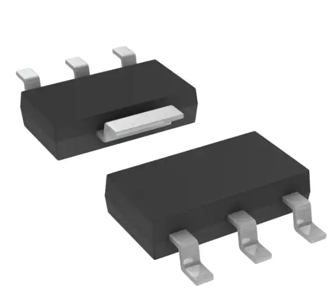
AMS1117is available in SOT-223, TO-252,SOT-89
Se
can provide an output voltage from 1.25 to 12V with only
two external resistors.
1%.
power package.
mi
Typical Application
co
r
to
uc
nd
Application circuit of AMS1117fixed version
Typical Electrical Characteristic
www.jsmsemi.com
第1/10页
�AMS1117系列
800mA Bipolar Linear Regulator
Selection Table
Marking
Part No.
Output Voltage
XX=12
1.2V
XX=18
1.8V
XX=28
2.85V
XX=25
2.5V
XX=33
3.3V
XX=50
5.0V
XX=AD
Adj
1117
XXYYWW
JS
MI
Designator
Description
1117
Product code
XX
Output Voltage(1.2~12.0V)
YYWW
DATE CODE
O
1117
XXYYWW
SOT-223
TO-252
SOT-89
CR
Ordering Information
Marking
Package
Temperature&Rohs
C:-40~85℃ ,Pb Free Rohs Std.
L:SOT-223
O:TO-252
co
Package type
Description
mi
Parameters
Se
Note:”XX” stands for output voltages. Other voltages can be specially customized
TR:Tape&Reel (Standard)
Voltage accuracy
2%(Customized)
r
to
uc
nd
Packing type:
Block Diagram
Pin Configuration
www.jsmsemi.com
第2/10页
�AMS1117系列
800mA Bipolar Linear Regulator
JS
Absolute Maximum Ratings
Max Input Voltage··················································································· ······················ ·· 30V
MI
Max Operating Junction Temperature(Tj)····················································· ······················ ·· 150℃
Ambient Temperature(Ta)······························································································· ·· -40℃~ 85℃
CR
Storage Temperature(Ts)········································································· ······················ ·· -40℃~150℃
Lead Temperature & Time········································································ ······················ ·· 260℃ 10S
device reliability.
O
Caution: Exceed these limits to damage to the device. Exposure to absolute maximum rating conditions may affect
Se
Recommended Work Conditions
Recommended maximum input voltage··········································································· ········
mi
Recommended operating junction temperature(Tj)·····································································
SOT-223
Rating
Unit
20
℃/W
12.5
SOT89
200
www.jsmsemi.com
-20~125℃
℃/W
℃/W
r
to
uc
TO-252
nd
Package thermal
resistance
co
Thermal Information
Parameter
Package
15V
第3/10页
�AMS1117系列
800mA Bipolar Linear Regulator
Electrical Characteristics
TA=25℃,unless otherwise noted.
Symbol
Parameter
Vref
Reference
voltage
Conditions
AMS1117-Adj
Min
Typ
Max
Unit
1.225
1.25
1.275
V
1.176
1.2
1.224
V
1.764
1.8
1.836
V
2.45
2.5
2.55
V
2.793
2.85
2.907
V
3.234
3.3
3.366
V
4.9
5
5.1
V
0.03
0.2
%/V
0.03
0.2
%/V
0.03
0.2
%/V
0.03
0.2
%/V
10mA≤Iout≤800mA , Vin=3.25V
AMS1117-1.2V
0≤Iout≤800mA , Vin=3.2V
AMS1117-1.8V
0≤Iout≤800mA , Vin=3.8V
JS
Vout
AMS1117-2.5V
Output voltage
0≤Iout≤800mA , Vin=4.5V
MI
AMS1117-2.85V
0≤Iout≤800mA , Vin=4.85V
CR
AMS1117-3.3V
0≤Iout≤800mA , Vin=5.3V
O
AMS1117-5.0V
0≤Iout≤800mA , Vin=7.0V
Se
AMS1117-1.2V
AMS1117-ADJ
Iout=10mA, 2.75V≤Vin≤12V
AMS1117-1.8V
Iout=10mA, 3.3V≤Vin≤12V
Line
regulation
AMS1117-2.5V
Iout=10mA, 4.0V≤Vin≤12V
AMS1117-2.85V
Iout=10mA, 4.35V≤Vin≤12V
AMS1117-3.3V
Iout=10mA, 4.8V≤Vin≤12V
AMS1117-5.0V
Iout=10mA, 6.5V≤Vin≤12V
AMS1117-1.2V
r
to
uc
nd
△Vout
co
mi
Iout=10mA, 2.7V≤Vin≤10V
0.03
0.2
%/V
0.03
0.2
%/V
0.03
0.2
%/V
2
8
mV
2
8
mV
3
12
mV
4
16
mV
Vin =2.7V, 10mA≤Iout≤800mA
AMS1117-ADJ
Vin =2.75V, 10mA≤Iout≤800mA
AMS1117-1.8V
Vin =3.3V, 10mA≤Iout≤800mA
△Vout
Load
regulation
AMS1117-2.5V
Vin =4.0V, 10mA≤Iout≤800mA
www.jsmsemi.com
第4/10页
�AMS1117系列
800mA Bipolar Linear Regulator
5
20
mV
6
24
mV
9
36
mV
Iout =100mA
1.2
1.3
V
Iout=800mA
1.3
1.5
V
AMS1117-ADJ
2
10
mA
AMS1117-1.2V,Vin=10V
2
5
mA
AMS1117-1.8V,Vin=12V
2
5
mA
AMS1117-2.5V,Vin=12V
2
5
mA
AMS1117-2.85V,Vin=12V
2
5
mA
AMS1117-3.3V,Vin=12V
2
5
mA
AMS1117-5.0V,Vin=12V
2
5
mA
AMS1117-ADJ
55
120
uA
0.2
10
uA
AMS1117-2.85V
Vin =4.35V, 10mA≤Iout≤800mA
AMS1117-3.3
Vin =4.8V, 10mA≤Iout≤800mA
AMS1117-5.0
Vin =6.5V, 10mA≤Iout≤800mA
Vdrop
Minimum load
JS
Imin
Dropout voltage
current
MI
Iq
Quiescent
Adjust pin
Ichange
Iadj change
Vin=5V,10mA≤Iout≤800mA
Se
current
O
IAdj
CR
Current
AMS1117-ADJ
ΔV/ΔT
Temperature
θJC
SOT-223
resistance
TO-252
20
nd
Thermal
ppm
±100
co
coefficien
mi
Vin=5V,10mA≤Iout≤800mA
10
℃/W
Note1: All test are conducted under ambient temperature 25°C and within a short period of time 20ms
r
to
uc
Note2: Load current smaller than minimum load current of AMS1117-ADJ will lead to unstable or oscillation output.
www.jsmsemi.com
第5/10页
�AMS1117系列
800mA Bipolar Linear Regulator
Detailed Description
AMS1117is a series of low dropout voltage, three terminal regulators. Its application circuit is very simple: the fixed
version only needs two capacitors and the adjustable version only needs two resistors and two capacitors to work. It is
composed of some modules including start-up circuit, bias circuit, bandgap, thermal shutdown, power transistors and its
driver circuit and so on.
The thermal shut down modules can assure chip and its application system working safety when the junction temperature
is larger than 140°C.
The bandgap module provides stable reference voltage, whose temperature coefficient is compensated by careful design
considerations. The temperature coefficient is under 100 ppm/°C. And the accuracy of output voltage is guaranteed by
JS
trimming technique.
MI
Typical Application
AMS1117has an adjustable version and six fixed versions (1.2V, 1.8V, 2.5V, 2.85V , 3.3V and 5V)
O
CR
Fixed Output Voltage Version
Se
Application circuit of AMS1117fixed version
mi
1)
Recommend using 10uF tan capacitor as bypass capacitor (C1) for all application circuit.
2)
Recommend using 10uF tan capacitor to assure circuit stability.
co
Adjustable Output Voltage Version
r
to
uc
nd
Application Circuit of AMS1117-ADJ
The output voltage of adjustable version follows the equation: Vout=1.25×(1+R2/R1)+IAdj×R2. We can ignore
IAdj because IAdj (about 50uA) is much less than the current of R1 (about 2~10mA).
1)
To meet the minimum load current (>10mA) requirement, R1 is recommended to be 125ohm or lower. As
HS1117C-ADJ can keep itself stable at load current about 2mA, R1 is not allowed to be higher than 625ohm.
2)
Using a bypass capacitor (CADJ) between the ADJ pin and ground can improve ripple rejection.
This bypass
capacitor prevents ripple from being amplified as the output voltage is increased. The impedance of CADJ should be less
than R1 to prevent ripple from being amplified. As R1 is normally in the range of
100Ω~500Ω,
the value of CADJ
should
satisfy this equation: 1/(2π×fripple×CADJ)


 工商网监
湘ICP备2023018690号
工商网监
湘ICP备2023018690号
