AGM30P10S
100% EAS Guaranteed
Green Device Available
Super Low Gate Charge
Excellent CdV/dt effect decline
Advanced high cell density Trench
technology
Product Summary
BVDSS
RDSON
-30V
ID
12mΩ
-14A
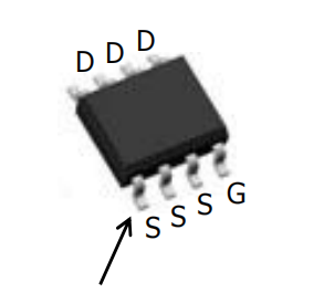
SOP-8 Pin Configuration
D
DD
Description
AGM30P10S is the high cell density
trenched P-ch MOSFETs, which provide
excellentRDSON and gate charge for most
of the synchronous buck converter
applications.
S G
S
S
Package Marking and Ordering Information
Device Marking
Device
AGM30P10S
AGM30P10S
Device Package
3000
---mm
---mm
SOP-8
Quantity
Tape width
Reel Size
●Absolute Maximum Ratings(TC =25℃)
Parameter
Symbol
Rating
Unit
Drain-Source Voltage
VDS
-30
V
Gate-Source Voltage
VGS
±20
V
ID
-14
A
IDM
-30
A
PD@TC=25℃
3.6
W
PD@TA=25℃
0.69
W
TJ
-55 to 150
℃
Storage Temperature
TSTG
-55 to 150
℃
Single Pulse Avalanche Energy
EAS
100
mJ
Continuous Drain Current(TC=25℃)
①
Pulsed Drain Current
Total Power Dissipation
②
Total Power Dissipation
Operating Junction Temperature
●Thermal resistance
Symbol
Min.
Typ.
Max.
Unit
Thermal resistance, junction - case
RthJC
-
-
34
°C/W
Thermal resistance, junction - ambient
RthJA
-
-
180
°C/W
Soldering temperature, wavesoldering for 10s
Tsold
-
-
265
°C
Parameter
②
www.agm-mos.com
1
VER2.5
�AGM30P10S
●Electronic Characteristics
Parameter
Symbol
Condition
Min.
Drain-Source Breakdown
Voltage
BVDSS
VGS =0V,ID =-250uA
-30
Gate Threshold Voltage
VGS(TH)
VGS =V DS, ID =-250uA
-1.2
Drain-Source Leakage Current
IDSS
Gate- Source Leakage Current
IGSS
Static Drain-source On
Resistance
RDS(ON)
Forward Transconductance
gFS
Typ
Max.
Unit
V
-2.5
V
VDS=-30V, VGS =0V
-1.0
uA
VGS=±12V ,VDS =0V
±100
nA
16
mΩ
VGS=-10V, ID=-9A
12
VGS=-4.5V, ID=-8A
18
VDS =-10V, ID=-5A
9
23
mΩ
s
●Electronic Characteristics
Parameter
Symbol
Input capacitance
Ciss
Output capacitance
Coss
Reverse transfer capacitance
Crss
Condition
f = 1MHz
Min.
Typ
Max.
-
1650
-
-
330
-
-
220
-
Unit
pF
●Gate Charge characteristics(Ta = 25℃)
Parameter
Symbol
Condition
Min.
Typ
Max.
Total gate charge
Qg
VDD =25V
-
15
-
Gate - Source charge
Qgs
ID = 8A
-
4
-
Gate - Drain charge
Qgd
VGS = 10V
-
6
-
Unit
nC
Note: ① Pulse Test : Pulse width ≤ 300μs, Duty cycle ≤ 2% ;
② Device mounted on FR-4 substrate PC board, 2oz copper, with thermal bias to bottom
layer 1inch square copper plate;
www.agm-mos.com
2
VER2.5
�AGM30P10S
Fig.1 Power Dissipation Derating Curve
Fig.2 Typical output Characteristics
50
1
VGS=-10V
40
Drain Current (A)
Power Dissipation Pd/Pd MAX.%
1.2
0.8
0.6
0.4
30
VGS=-4.5V
20
10
0.2
0
0
0
0
50
100
150
Temperature (。C)
Junction Temperature
50
1
Drain-Source voltage (V)
200
Fig.3 Threshold Voltage V.S Junction Temperature
-50
0.5
Fig.4 Resistance V.S Drain Current
30
150
ON Resistance
0
Vgs(th )d
-0.5
-1
20
10
-1.5
0
-2
0
20
30
40
Drain Current(A)
-2.5
Fig.5 On-Resistance VS Gate Source Voltage
Fig.6 On-Resistance V.S Junction Temperature
30
1.5
Normalized ON-Resistance
RDson(mΩ)
10
20
10
0
1
0.5
3
5
7
9
-50
VGS( -V )
www.agm-mos.com
0
50
100
150
Temperature
3
VER2.5
�AGM30P10S
Fig.7 Switching Time Measurement Circuit
Fig.8 Gate Charge Waveform
Fig.9 Switching Time Measurement Circuit
Fig.10 Gate Charge Waveform
Fig.11 Avalanche Measurement Circuit
www.agm-mos.com
Fig.12 Avalanche Waveform
4
VER2.5
�AGM30P10S
●Dimensions(SOP8)
SYMBOL
min
A
A1
TYP
max
SYMBOL
min
max
4.80
5.00
C
1.30
1.50
0.37
0.47
C1
0.55
0.75
A2
1.27
C2
0.55
0.65
A3
0.41
C3
0.05
0.20
0.19
B
5.80
6.20
C4
B1
3.80
4.00
D
B2
www.agm-mos.com
5.00
D1
5
0.20
0.23
1.05
0.40
0.62
VER2.5
�AGM30P10S
Disclaimers:
Information furnished in this document is believed to be accurate and reliable.
However,
Shenzhen Core Control Source Semiconductor Co., Ltd. assumes no responsibility for
the consequences of
use without consideration for such information nor use beyond it.
Information mentioned in this document is subject to change without notice, apart from
that
when an agreement is signed, Shenzhen core control source complies with the
agreement.
Products and information provided in this document have no infringement of patents.
Shenzhen Core Control Source Semiconductor Co., Ltd. assumes no responsibility for
any infringement of other rights of third parties which may
result from the use of such products and information.
This document is the first version which is made in 12-Apr-20. This document
supersedes and
replaces all information previously supplied.
is a registered trademark of Shenzhen Core Control Source
Semiconductor Co., Ltd.
Copyright ©2017 Shenzhen Core Control Source Semiconductor Co., Ltd. Printed All
rights reserved.
www.agm-mos.com
6
VER2.5
�
很抱歉,暂时无法提供与“AGM30P10S”相匹配的价格&库存,您可以联系我们找货
免费人工找货- 国内价格
- 1+0.54000
- 10+0.52000
- 100+0.47200
- 500+0.44800