AGM30P10AP
Product Summary
100% EAS Guaranteed
Green Device Available
Super Low Gate Charge
Excellent CdV/dt effect decline
Advanced high cell density Trench
technology
BVDSS
RDSON
-30V
ID
11mΩ
-23A
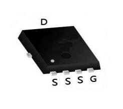
PRPAK3.3X3.3 Pin Configuration
Description
AGM30P10AP is the high cell density
trenched P-ch MOSFETs, which provide
excellent
RDSON and gate charge for most
of the synchronous buck converter
applications.
Package Marking and Ordering Information
Device Marking
Device
AGM30P10AP
AGM30P10AP
Device Package
Reel Size
DFN3.3*3.3
Tape width
--mm
Quantity
--mm
5000
Table 1. Absolute Maximum Ratings (TA=25℃)
Symbol
Parameter
VDS
Drain-Source Voltage (VGS=0V)
VGS
Gate-Source Voltage (VDS=0V)
Value
-30
±20
Unit
V
V
Drain Current-Continuous(Tc=25℃) (Note 1)
-23
A
Drain Current-Continuous(Tc=100℃)
-19
A
-62
A
ID
IDM (pluse)
Drain Current-Continuous@ Current-Pulsed (Note 2)
Maximum Power Dissipation(T c=25℃)
37
W
Maximum Power Dissipation(T c=100℃)
27
W
Avalanche energy (Note 3)
75
mJ
-55 To 150
℃
PD
EAS
TJ,TSTG
Operating Junction and Storage Temperature Range
Table 2. Thermal Characteristic
Symbol
RθJA
RθJC
www.agm-mos.com
Parameter
Typ
Thermal Resistance Junction-ambient (Steady State)1
Thermal Resistance Junction-Case1
1
Max
Unit
---
70
℃/W
---
3.4
℃/W
VER2.5
�AGM30P10AP
Table 3. Electrical Characteristics (TA=25℃unless otherwise noted)
Symbol
Parameter
Conditions
Min
Typ
Max
Unit
On/Off States
BVDSS
Drain-Source Breakdown Voltage
IDSS
Zero Gate Voltage Drain Current
IGSS
Gate-Body Leakage Current
VGS(th)
gFS
RDS(ON)
VGS=0V ID=250μA
-30
V
VDS=-24V,VGS=0V
-1
VGS=±20V,VDS=0V
Gate Threshold Voltage
VDS=VGS,ID=250μA
Forward Transconductance
Drain-Source On-State Resistance
1.2
1.3
VDS=-5V,ID=-20A
30
VGS=-10V, ID=-20A
11
μA
±100
nA
2.1
V
S
13.9
mΩ
mΩ
VGS=-4.5V, ID=-15A
Dynamic Characteristics
Ciss
Input Capacitance
Coss
Output Capacitance
Crss
Rg
VDS=-15V,
VGS=0V,
F=1MHZ
Reverse Transfer Capacitance
Gate resistance
1380
pF
310
pF
pF
237
VGS=0V, VDS=0V,f=1.0MHz
Ω
9
Switching Times
8
nS
73
nS
Turn-Off Delay Time
61.8
nS
tf
Turn-Off Fall Time
24.4
nS
Qg
Total Gate Charge
22
nC
Qgs
Gate-Source Charge
8.7
nC
Qgd
Gate-Drain Charge
7.2
nC
td(on)
Turn-on Delay Time
tr
Turn-on Rise Time
td(off)
VGS=-10V,
VDD=-15V,
ID=-15A,RGEN=3.3
VGS=-10V, VDS=-25V, ID=-12A
Source-Drain Diode Characteristics
-23
A
VGS=0V,IS=-1A
1.0
V
Reverse Recovery Time
IF=-15A , dI/dt=100A/µs ,
19
ns
Reverse Recovery Charge
·TJ=25℃
9
nc
IS
Continuous Source Current
VSD
Forward on Voltage
trr
Qrr
VG=VD=0V , Force Current
Notes 1.The maximum current rating is package limited.
Notes 2.Repetitive Rating: Pulse width limited by maximum junction temperature
Notes 3.EAS condition: TJ=25℃,VDD=15V,VG=10V, RG=25Ω
www.agm-mos.com
2
VER2.5
�AGM30P10AP
Typical Characteristics
150
-ID Drain Current (A)
125
VGS=-10V
VGS=-7V
100
75
VGS=-5V
50
VGS=-4.5V
VGS=-3V
25
0
0
0.5
1
1.5
2
2.5
3
3.5
4
-VDS , Drain-to-Source Voltage (V)
Fig.1 Typical Output Characteristics
Fig.2 On-Resistance vs. G-S Voltage
12
10
-VGS Gate to Source Voltage (V)
-IS Source Current(A)
VDS=-15V
8
TJ=150℃
TJ=25℃
4
0
0.00
0.25
0.50
0.75
ID=-15A
8
6
4
2
0
1.00
0
-VSD , Source-to-Drain Voltage (V)
18
27
36
45
QG , Total Gate Charge (nC)
Fig.4 Gate-Charge Characteristics
Fig.3 Forward Characteristics of Reverse
2.0
Normalized On Resistance
1.5
Normalized VGS(th)
9
1.5
1
1.0
0.5
0.5
0
-50
0
50
100
TJ ,Junction Temperature (℃ )
-50
150
Fig.5 Normalized VGS(th) vs. TJ
www.agm-mos.com
0
50
100
150
TJ , Junction Temperature (℃)
Fig.6 Normalized RDSON vs. TJ
3
VER2.5
�AGM30P10AP
1000.00
10000
F=1.0MHz
10us
Ciss
100us
1000
10.00
-ID (A)
Capacitance (pF)
100.00
Coss
1.00
Crss
100
1ms
10ms
100ms
DC
0.10
TC=25℃
Single Pulse
0.01
10
1
5
9
13
17
21
0.1
25
1
10
100
-VDS (V)
-VDS , Drain to Source Voltage (V)
Fig.7 Capacitance
Fig.8 Safe Operating Area
Normalized Thermal Response (RθJC)
1
DUTY=0.5
0.2
0.1
0.1
0.05
0.02
0.01
0.01
PDM
SINGLE PULSE
TON
T
D = TON/T
TJpeak = TC + PDM x RθJC
0.001
0.00001
0.0001
0.001
0.01
0.1
1
10
t , Pulse Width (s)
Fig.9 Normalized Maximum Transient Thermal Impedance
Fig.10 Switching Time Waveform
www.agm-mos.com
Fig.11 Unclamped Inductive Switching Waveform
4
VER2.5
�AGM30P10AP
PDFN3333 Package Outline Data
DIMENSIONS ( unit : mm )
Symbol
Min
Typ
Max
Symbol
Min
Typ
Max
A
0.70
0.75
0.80
b
0.25
0.30
0.35
C
0.10
0.15
0.25
D
3.25
3.35
3.45
D1
3.00
3.10
3.20
D2
1.78
1.88
1.98
D3
--
0.13
--
E
3.20
3.30
3.40
E1
3.00
3.15
3.20
E2
2.39
2.49
2.59
H
0.30
0.39
0.50
0.65BSC
e
L
0.30
0.40
0.50
L1
--
0.13
--
θ
--
10°
12°
M
*
*
0.15
*Not specified
www.agm-mos.com
5
VER2.5
�AGM30P10AP
Disclaimers:
Information furnished in this document is believed to be accurate and reliable.
However,
Shenzhen Core Control Source Semiconductor Co., Ltd. assumes no responsibility for
the consequences of
use without consideration for such information nor use beyond it.
Information mentioned in this document is subject to change without notice, apart from
that
when an agreement is signed, Shenzhen core control source complies with the
agreement.
Products and information provided in this document have no infringement of patents.
Shenzhen Core Control Source Semiconductor Co., Ltd. assumes no responsibility for
any infringement of other rights of third parties which may
result from the use of such products and information.
This document is the first version which is made in 12-Apr-18. This document
supersedes and
replaces all information previously supplied.
is a registered trademark of Shenzhen Core Control Source
Semiconductor Co., Ltd.
Copyright ©2017 Shenzhen Core Control Source Semiconductor Co., Ltd. Printed All
rights reserved.
www.agm-mos.com
6
VER2.5
�
很抱歉,暂时无法提供与“AGM30P10AP”相匹配的价格&库存,您可以联系我们找货
免费人工找货- 国内价格
- 1+0.72000
- 100+0.67200
- 300+0.62400
- 500+0.57600
- 2000+0.55200
- 5000+0.53760