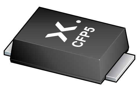
PMEG6020EP
2 A low VF MEGA Schottky barrier rectifier
28 February 2019
Product data sheet
1. General description
Planar Maximum Efficiency General Application (MEGA) Schottky barrier rectifier with an integrated
guard ring for stress protection, encapsulated in a SOD128 small and flat lead Surface-Mounted
Device (SMD) plastic package.
2. Features and benefits
•
•
•
•
•
•
•
Average forward current: IF(AV) ≤ 2 A
Reverse voltage: VR ≤ 60 V
Low forward voltage
High power capability due to clip-bond technology
AEC-Q101 qualified
Small and flat lead SMD plastic package
Capable for reflow and wave soldering
3. Applications
•
•
•
•
•
Low voltage rectification
High efficiency DC-to-DC conversion
Switch Mode Power Supply (SMPS)
Reverse polarity protection
Low power consumption applications
4. Quick reference data
Table 1. Quick reference data
Symbol
Parameter
IF(AV)
average forward
current
Conditions
Min
Typ
Max
Unit
-
-
2
A
δ = 0.5; f = 20 kHz; Tsp ≤ 140 °C;
square wave
-
-
2
A
δ = 0.5; f = 20 kHz; Tamb ≤ 85 °C;
square wave
[1]
VR
reverse voltage
Tj = 25 °C
-
-
60
V
VF
forward voltage
IF = 2 A; Tj = 25 °C
-
460
530
mV
IR
reverse current
VR = 60 V; Tj = 25 °C
-
60
150
µA
[1]
Device mounted on a ceramic PCB, Al2O3, standard footprint.
�PMEG6020EP
Nexperia
2 A low VF MEGA Schottky barrier rectifier
5. Pinning information
Table 2. Pinning information
Pin
Symbol Description
1
K
cathode[1]
2
A
anode
Simplified outline
1
Graphic symbol
2
K
A
sym001
CFP5 (SOD128)
[1]
The marking bar indicates the cathode.
6. Ordering information
Table 3. Ordering information
Type number
Package
PMEG6020EP
Name
Description
Version
CFP5
plastic, surface mounted package; 2 terminals; 4 mm pitch; 3.8
mm x 2.6 mm x 1 mm body
SOD128
7. Marking
Table 4. Marking codes
Type number
Marking code
PMEG6020EP
AA
PMEG6020EP
Product data sheet
All information provided in this document is subject to legal disclaimers.
28 February 2019
©
Nexperia B.V. 2019. All rights reserved
2 / 13
�PMEG6020EP
Nexperia
2 A low VF MEGA Schottky barrier rectifier
8. Limiting values
Table 5. Limiting values
In accordance with the Absolute Maximum Rating System (IEC 60134).
Symbol
Parameter
Conditions
Min
Max
Unit
VR
reverse voltage
Tj = 25 °C
-
60
V
IF(AV)
average forward current
δ = 0.5; f = 20 kHz; Tamb ≤ 85 °C; square
wave
-
2
A
δ = 0.5; f = 20 kHz; Tsp ≤ 140 °C; square
wave
-
2
A
-
50
A
[2]
-
625
mW
[3]
-
1.05
W
[1]
-
2.1
W
IFSM
non-repetitive peak
forward current
tp = 8 ms; square wave; Tj(init) = 25 °C
Ptot
total power dissipation
Tamb ≤ 25 °C
[1]
Tj
junction temperature
-
150
°C
Tamb
ambient temperature
-55
150
°C
Tstg
storage temperature
-65
150
°C
[1]
[2]
[3]
Device mounted on a ceramic PCB, Al2O3, standard footprint.
Device mounted on an FR4 PCB, single-sided copper, tin-plated and standard footprint.
2
Device mounted on an FR4 PCB, single-sided copper, tin-plated, mounting pad for cathode 1 cm .
9. Thermal characteristics
Table 6. Thermal characteristics
Symbol
Parameter
Rth(j-a)
Rth(j-sp)
[1]
[2]
[3]
[4]
[5]
Conditions
thermal resistance from in free air
junction to ambient
thermal resistance from
junction to solder point
Min
Typ
Max
Unit
[1] [2]
-
-
200
K/W
[1] [3]
-
-
120
K/W
[1] [4]
-
-
60
K/W
[5]
-
-
12
K/W
For Schottky barrier diodes thermal runaway has to be considered, as in some applications the reverse power losses PR are a
significant part of the total power losses.
Device mounted on an FR4 PCB, single-sided copper, tin-plated and standard footprint.
2
Device mounted on an FR4 PCB, single-sided copper, tin-plated, mounting pad for cathode 1 cm .
Device mounted on a ceramic PCB, Al2O3, standard footprint.
Soldering point of cathode tab.
PMEG6020EP
Product data sheet
All information provided in this document is subject to legal disclaimers.
28 February 2019
©
Nexperia B.V. 2019. All rights reserved
3 / 13
�PMEG6020EP
Nexperia
2 A low VF MEGA Schottky barrier rectifier
006aab678
103
Zth(j-a)
(K/W)
duty cycle =
1
102
0.75
0.5
0.33
0.2
0.25
0.1
10
0.05
0.02
1
0.01
0
10- 1
10- 3
10- 2
10- 1
1
10
102
tp (s)
103
FR4 PCB, standard footprint
Fig. 1.
Transient thermal impedance from junction to ambient as a function of pulse duration; typical values
006aab679
103
Zth(j-a)
(K/W)
duty cycle =
1
102
0.75
0.5
0.33
0.25
0.2
0.1
10
0.05
0.02
1
0.01
0
10- 1
10- 3
10- 2
10- 1
FR4 PCB, mounting pad for cathode 1 cm
Fig. 2.
1
10
102
tp (s)
2
103
Transient thermal impedance from junction to ambient as a function of pulse duration; typical values
102
006aab680
duty cycle =
1
Zth(j-a)
(K/W)
0.5
10
0.25
0.75
0.33
0.2
0.1
0.05
0.02
0.01
1
0
10- 1
10- 3
10- 2
10- 1
1
10
102
tp (s)
103
Ceramic PCB, Al2O3, standard footprint
Fig. 3.
Transient thermal impedance from junction to ambient as a function of pulse duration; typical values
PMEG6020EP
Product data sheet
All information provided in this document is subject to legal disclaimers.
28 February 2019
©
Nexperia B.V. 2019. All rights reserved
4 / 13
�PMEG6020EP
Nexperia
2 A low VF MEGA Schottky barrier rectifier
10. Characteristics
Table 7. Characteristics
Symbol
Parameter
Conditions
Min
Typ
Max
Unit
VF
IF = 0.1 A; Tj = 25 °C
-
300
340
mV
IF = 0.5 A; Tj = 25 °C
-
360
420
mV
IF = 1 A; Tj = 25 °C
-
400
460
mV
IF = 1.5 A; Tj = 25 °C
-
430
500
mV
IF = 2 A; Tj = 25 °C
-
460
530
mV
VR = 5 V; Tj = 25 °C
-
2.5
-
µA
VR = 10 V; Tj = 25 °C
-
3.5
-
µA
VR = 60 V; Tj = 25 °C
-
60
150
µA
VR = 1 V; f = 1 MHz; Tj = 25 °C
-
240
-
pF
VR = 10 V; f = 1 MHz; Tj = 25 °C
-
80
-
pF
forward voltage
IR
reverse current
Cd
diode capacitance
006aab872
10
IF
(A)
(1)
1
(2)
006aab873
10- 1
IR
(A)
10- 2
(1)
(2)
10- 3
10- 1
10- 4
(3)
(4)
(5)
(3)
10- 5
10- 2
10- 6
10- 3
10- 4
10- 7
0
0.2
0.4
0.6
VF (V)
0.8
(1) Tj = 150 °C
(2) Tj = 125 °C
(3) Tj = 85 °C
(4) Tj = 25 °C
(5) Tj = −40 °C
Fig. 4.
Product data sheet
0
20
40
VR (V)
60
(1) Tj = 125 °C
(2) Tj = 85 °C
(3) Tj = 25 °C
(4) Tj = −40 °C
Forward current as a function of forward
voltage; typical values
PMEG6020EP
10- 8
(4)
Fig. 5.
Reverse current as a function of reverse
voltage; typical values
All information provided in this document is subject to legal disclaimers.
28 February 2019
©
Nexperia B.V. 2019. All rights reserved
5 / 13
�PMEG6020EP
Nexperia
2 A low VF MEGA Schottky barrier rectifier
006aab874
500
006aab875
1.4
PF(AV)
(W)
1.2
Cd
(pF)
400
(4)
(3)
1.0
300
0.8
(2)
(1)
0.6
200
0.4
100
0
0.2
0
20
40
VR (V)
0.0
60
f = 1 MHz; Tamb = 25 °C
Fig. 6.
1
2
IF(AV) (A)
Fig. 7.
006aab876
Average forward power dissipation as a
function of average forward current; typical
values
006aab877
3.0
PR(AV)
(W)
3
Tj = 150 °C
(1) δ = 0.1
(2) δ = 0.2
(3) δ = 0.5
(4) δ = 1
Diode capacitance as a function of reverse
voltage; typical values
2.0
0
IF(AV)
(A)
1.6
(1)
2.0
1.2
(2)
(1)
0.8
(2)
(3)
1.0
(3)
(4)
0.4
0.0
(4)
0
20
40
VR (V)
0.0
60
Tj = 125 °C
(1) δ = 1
(2) δ = 0.9
(3) δ = 0.8
(4) δ = 0.5
Fig. 8.
Average reverse power dissipation as a
function of reverse voltage; typical values
PMEG6020EP
Product data sheet
0
25
50
75
100
125
150
175
Tamb (°C)
FR4 PCB, standard footprint
Tj = 150 °C
(1) δ = 1; DC
(2) δ = 0.5; f = 20 kHz
(3) δ = 0.2; f = 20 kHz
(4) δ = 0.1; f = 20 kHz
Fig. 9.
Average forward current as a function of
ambient temperature; typical values
All information provided in this document is subject to legal disclaimers.
28 February 2019
©
Nexperia B.V. 2019. All rights reserved
6 / 13
�PMEG6020EP
Nexperia
2 A low VF MEGA Schottky barrier rectifier
006aab878
3.0
(1)
IF(AV)
(A)
2.0
(1)
IF(AV)
(A)
2.0
(2)
(2)
(3)
(3)
1.0
006aab879
3.0
1.0
(4)
0.0
0
25
(4)
50
75
100
125
0.0
150
175
Tamb (°C)
2
FR4 PCB, mounting pad for cathode 1 cm
Tj = 150 °C
(1) δ = 1; DC
(2) δ = 0.5; f = 20 kHz
(3) δ = 0.2; f = 20 kHz
(4) δ = 0.1; f = 20 kHz
0
25
50
75
100
125
150
175
Tamb (°C)
Ceramic PCB, Al2O3, standard footprint
Tj = 150 °C
(1) δ = 1; DC
(2) δ = 0.5; f = 20 kHz
(3) δ = 0.2; f = 20 kHz
(4) δ = 0.1; f = 20 kHz
Fig. 10. Average forward current as a function of
ambient temperature; typical values
Fig. 11. Average forward current as a function of
ambient temperature; typical values
006aab880
3.0
(1)
IF(AV)
(A)
2.0
(2)
(3)
1.0
(4)
0.0
0
25
50
75
100
125
150
175
Tsp (°C)
Tj = 150 °C
(1) δ = 1; DC
(2) δ = 0.5; f = 20 kHz
(3) δ = 0.2; f = 20 kHz
(4) δ = 0.1; f = 20 kHz
Fig. 12. Average forward current as a function of solder point temperature; typical values
PMEG6020EP
Product data sheet
All information provided in this document is subject to legal disclaimers.
28 February 2019
©
Nexperia B.V. 2019. All rights reserved
7 / 13
�PMEG6020EP
Nexperia
2 A low VF MEGA Schottky barrier rectifier
11. Test information
P
t2
duty cycle δ =
t1
t2
t1
t
006aaa812
Fig. 13. Duty cycle definition
The current ratings for the typical waveforms are calculated according to the equations: IF(AV)=IM×δ
with IM defined as peak current, IRMS=IF(AV) at DC, and IRMS=IM×√δ with IRMS defined as RMS
current.
Quality information
This product has been qualified in accordance with the Automotive Electronics Council (AEC)
standard Q101 - Stress test qualification for discrete semiconductors, and is suitable for use in
automotive applications.
12. Package outline
2.7
2.3
1.1
0.9
0.6
0.3
1
5.0
4.4
4.0
3.6
2
1.9
1.6
0.22
0.10
Dimensions in mm
07-09-12
Fig. 14. Package outline CFP5 (SOD128)
PMEG6020EP
Product data sheet
All information provided in this document is subject to legal disclaimers.
28 February 2019
©
Nexperia B.V. 2019. All rights reserved
8 / 13
�PMEG6020EP
Nexperia
2 A low VF MEGA Schottky barrier rectifier
13. Soldering
6.2
4.4
4.2
solder lands
1.9 2.1
(2×) (2×)
3.4 2.5
solder resist
solder paste
occupied area
Dimensions in mm
1.2
(2×)
1.4
(2×)
sod128_fr
Fig. 15. Reflow soldering footprint for CFP5 (SOD128)
PMEG6020EP
Product data sheet
All information provided in this document is subject to legal disclaimers.
28 February 2019
©
Nexperia B.V. 2019. All rights reserved
9 / 13
�PMEG6020EP
Nexperia
2 A low VF MEGA Schottky barrier rectifier
Wave soldering footprint information
SOD128
10.2
5.8
2.3
5.7
4.2
(2×)
4.35
(2×)
3.5 (2×)
3.65 (2×)
occupied area
solder resist
solder lands
dummy track (solder resist and Cu free)
Dimensions in mm
Issue date
17-06-06
17-06-07
sod128_fw
Fig. 16. Wave soldering footprint for CFP5 (SOD128)
PMEG6020EP
Product data sheet
All information provided in this document is subject to legal disclaimers.
28 February 2019
©
Nexperia B.V. 2019. All rights reserved
10 / 13
�PMEG6020EP
Nexperia
2 A low VF MEGA Schottky barrier rectifier
14. Revision history
Table 8. Revision history
Data sheet ID
Release date
Data sheet status
Change notice
Supersedes
PMEG6020EP v.2
20190228
Product data sheet
-
PMEG6020EP_1
Modifications:
•
•
PMEG6020EP_1
20100317
PMEG6020EP
Product data sheet
Features and benefits: Capable for reflow and wave soldering added
Soldering: Wave soldering footprint added
Product data sheet
-
All information provided in this document is subject to legal disclaimers.
28 February 2019
-
©
Nexperia B.V. 2019. All rights reserved
11 / 13
�PMEG6020EP
Nexperia
2 A low VF MEGA Schottky barrier rectifier
equipment, nor in applications where failure or malfunction of an Nexperia
product can reasonably be expected to result in personal injury, death or
severe property or environmental damage. Nexperia and its suppliers accept
no liability for inclusion and/or use of Nexperia products in such equipment or
applications and therefore such inclusion and/or use is at the customer's own
risk.
15. Legal information
Data sheet status
Document status
[1][2]
Product
status [3]
Definition
Quick reference data — The Quick reference data is an extract of the
product data given in the Limiting values and Characteristics sections of this
document, and as such is not complete, exhaustive or legally binding.
Objective [short]
data sheet
Development
This document contains data from
the objective specification for
product development.
Preliminary [short]
data sheet
Qualification
This document contains data from
the preliminary specification.
Applications — Applications that are described herein for any of these
products are for illustrative purposes only. Nexperia makes no representation
or warranty that such applications will be suitable for the specified use
without further testing or modification.
Product [short]
data sheet
Production
This document contains the product
specification.
[1]
[2]
[3]
Please consult the most recently issued document before initiating or
completing a design.
The term 'short data sheet' is explained in section "Definitions".
The product status of device(s) described in this document may have
changed since this document was published and may differ in case of
multiple devices. The latest product status information is available on
the internet at https://www.nexperia.com.
Definitions
Draft — The document is a draft version only. The content is still under
internal review and subject to formal approval, which may result in
modifications or additions. Nexperia does not give any representations or
warranties as to the accuracy or completeness of information included herein
and shall have no liability for the consequences of use of such information.
Short data sheet — A short data sheet is an extract from a full data sheet
with the same product type number(s) and title. A short data sheet is
intended for quick reference only and should not be relied upon to contain
detailed and full information. For detailed and full information see the relevant
full data sheet, which is available on request via the local Nexperia sales
office. In case of any inconsistency or conflict with the short data sheet, the
full data sheet shall prevail.
Product specification — The information and data provided in a Product
data sheet shall define the specification of the product as agreed between
Nexperia and its customer, unless Nexperia and customer have explicitly
agreed otherwise in writing. In no event however, shall an agreement be
valid in which the Nexperia product is deemed to offer functions and qualities
beyond those described in the Product data sheet.
Disclaimers
Limited warranty and liability — Information in this document is believed
to be accurate and reliable. However, Nexperia does not give any
representations or warranties, expressed or implied, as to the accuracy
or completeness of such information and shall have no liability for the
consequences of use of such information. Nexperia takes no responsibility
for the content in this document if provided by an information source outside
of Nexperia.
In no event shall Nexperia be liable for any indirect, incidental, punitive,
special or consequential damages (including - without limitation - lost
profits, lost savings, business interruption, costs related to the removal
or replacement of any products or rework charges) whether or not such
damages are based on tort (including negligence), warranty, breach of
contract or any other legal theory.
Customers are responsible for the design and operation of their applications
and products using Nexperia products, and Nexperia accepts no liability for
any assistance with applications or customer product design. It is customer’s
sole responsibility to determine whether the Nexperia product is suitable
and fit for the customer’s applications and products planned, as well as
for the planned application and use of customer’s third party customer(s).
Customers should provide appropriate design and operating safeguards to
minimize the risks associated with their applications and products.
Nexperia does not accept any liability related to any default, damage, costs
or problem which is based on any weakness or default in the customer’s
applications or products, or the application or use by customer’s third party
customer(s). Customer is responsible for doing all necessary testing for the
customer’s applications and products using Nexperia products in order to
avoid a default of the applications and the products or of the application or
use by customer’s third party customer(s). Nexperia does not accept any
liability in this respect.
Limiting values — Stress above one or more limiting values (as defined in
the Absolute Maximum Ratings System of IEC 60134) will cause permanent
damage to the device. Limiting values are stress ratings only and (proper)
operation of the device at these or any other conditions above those
given in the Recommended operating conditions section (if present) or the
Characteristics sections of this document is not warranted. Constant or
repeated exposure to limiting values will permanently and irreversibly affect
the quality and reliability of the device.
Terms and conditions of commercial sale — Nexperia products are
sold subject to the general terms and conditions of commercial sale, as
published at http://www.nexperia.com/profile/terms, unless otherwise agreed
in a valid written individual agreement. In case an individual agreement is
concluded only the terms and conditions of the respective agreement shall
apply. Nexperia hereby expressly objects to applying the customer’s general
terms and conditions with regard to the purchase of Nexperia products by
customer.
No offer to sell or license — Nothing in this document may be interpreted
or construed as an offer to sell products that is open for acceptance or the
grant, conveyance or implication of any license under any copyrights, patents
or other industrial or intellectual property rights.
Export control — This document as well as the item(s) described herein
may be subject to export control regulations. Export might require a prior
authorization from competent authorities.
Translations — A non-English (translated) version of a document is for
reference only. The English version shall prevail in case of any discrepancy
between the translated and English versions.
Trademarks
Notice: All referenced brands, product names, service names and
trademarks are the property of their respective owners.
Notwithstanding any damages that customer might incur for any reason
whatsoever, Nexperia’s aggregate and cumulative liability towards customer
for the products described herein shall be limited in accordance with the
Terms and conditions of commercial sale of Nexperia.
Right to make changes — Nexperia reserves the right to make changes
to information published in this document, including without limitation
specifications and product descriptions, at any time and without notice. This
document supersedes and replaces all information supplied prior to the
publication hereof.
Suitability for use in automotive applications — This Nexperia product
has been qualified for use in automotive applications. Unless otherwise
agreed in writing, the product is not designed, authorized or warranted to
be suitable for use in life support, life-critical or safety-critical systems or
PMEG6020EP
Product data sheet
All information provided in this document is subject to legal disclaimers.
28 February 2019
©
Nexperia B.V. 2019. All rights reserved
12 / 13
�PMEG6020EP
Nexperia
2 A low VF MEGA Schottky barrier rectifier
Contents
1. General description...................................................... 1
2. Features and benefits.................................................. 1
3. Applications.................................................................. 1
4. Quick reference data....................................................1
5. Pinning information......................................................2
6. Ordering information....................................................2
7. Marking.......................................................................... 2
8. Limiting values............................................................. 3
9. Thermal characteristics............................................... 3
10. Characteristics............................................................ 5
11. Test information.......................................................... 8
12. Package outline.......................................................... 8
13. Soldering..................................................................... 9
14. Revision history........................................................11
15. Legal information......................................................12
©
Nexperia B.V. 2019. All rights reserved
For more information, please visit: http://www.nexperia.com
For sales office addresses, please send an email to: salesaddresses@nexperia.com
Date of release: 28 February 2019
PMEG6020EP
Product data sheet
All information provided in this document is subject to legal disclaimers.
28 February 2019
©
Nexperia B.V. 2019. All rights reserved
13 / 13
�


 工商网监
湘ICP备2023018690号
工商网监
湘ICP备2023018690号

