Important notice
Dear Customer,
On 7 February 2017 the former NXP Standard Product business became a new company with the
tradename Nexperia. Nexperia is an industry leading supplier of Discrete, Logic and PowerMOS
semiconductors with its focus on the automotive, industrial, computing, consumer and wearable
application markets
In data sheets and application notes which still contain NXP or Philips Semiconductors references, use
the references to Nexperia, as shown below.
Instead of http://www.nxp.com, http://www.philips.com/ or http://www.semiconductors.philips.com/,
use http://www.nexperia.com
Instead of sales.addresses@www.nxp.com or sales.addresses@www.semiconductors.philips.com, use
salesaddresses@nexperia.com (email)
Replace the copyright notice at the bottom of each page or elsewhere in the document, depending on
the version, as shown below:
- © NXP N.V. (year). All rights reserved or © Koninklijke Philips Electronics N.V. (year). All rights
reserved
Should be replaced with:
- © Nexperia B.V. (year). All rights reserved.
If you have any questions related to the data sheet, please contact our nearest sales office via e-mail
or telephone (details via salesaddresses@nexperia.com). Thank you for your cooperation and
understanding,
Kind regards,
Team Nexperia
�DISCRETE SEMICONDUCTORS
DATA SHEET
k, halfpage
M3D087
BAT120 series
Schottky barrier double diodes
Product data sheet
Supersedes data of 2001 Aug 27
2003 Aug 04
�NXP Semiconductors
Product data sheet
Schottky barrier double diodes
BAT120 series
FEATURES
PINNING
• Low switching losses
BAT120
PIN
• Capability of absorbing very high surge current
• Fast recovery time
• Guard ring protected
• Plastic SMD package.
A
C
S
1
k1
a1
a1
2
n.c.
n.c.
n.c.
3
k2
a2
k2
4
a1, a2
k1, k2
k1, a2
APPLICATIONS
• Low power switched-mode power supplies
• Rectification
4
handbook, halfpage
• Polarity protection.
DESCRIPTION
Planar Schottky barrier double diodes encapsulated in a
SOT223 plastic SMD package.
MARKING
1
TYPE NUMBER
MARKING CODE
BAT120A
AT120A
BAT120C
AT120C
BAT120S
AT120S
3
MGL171
Simplified outline (SOT223) and pin
configuration.
a. BAT120A.
4
1
3
2 n.c.
MGL172
b. BAT120C.
Fig.2 BAT120 diode configurations and symbols.
2003 Aug 04
2
3
MSB002 - 1
4
1
2 n.c.
Top view
Fig.1
4
2
1
3
2 n.c.
c. BAT120S.
MGL173
�NXP Semiconductors
Product data sheet
Schottky barrier double diodes
BAT120 series
LIMITING VALUES
In accordance with the Absolute Maximum Rating System (IEC 60134).
SYMBOL
PARAMETER
CONDITIONS
MIN.
MAX.
UNIT
Per diode
−
25
V
−
1
A
−
10
A
−
0.5
A
storage temperature
−65
+150
°C
junction temperature
−
125
°C
operating ambient temperature
−65
+125
°C
VR
continuous reverse voltage
IF
continuous forward current
IFSM
non-repetitive peak forward current
tp < 10 ms; half sinewave;
JEDEC method
IRSM
non-repetitive peak reverse current
tp = 100 μs
Tstg
Tj
Tamb
ELECTRICAL CHARACTERISTICS
Tamb = 25 °C unless otherwise specified.
SYMBOL
PARAMETER
CONDITIONS
TYP.
MAX.
UNIT
Per diode
VF
IR
Cd
forward voltage
reverse current
diode capacitance
see Fig.3
IF = 100 mA
260
300
mV
IF = 1 A
400
450
mV
VR = 20 V; note 1; see Fig.4
80
500
μA
VR = 25 V; note 1; see Fig.4
−
1
mA
VR = 20 V; Tj = 100 °C; note 1
−
10
mA
f = 1 MHz; VR = 4 V; see Fig.5
100
−
pF
Note
1. Pulse test: tp = 300 μs; δ = 0.02.
THERMAL CHARACTERISTICS
SYMBOL
Rth j-a
PARAMETER
CONDITIONS
VALUE
UNIT
thermal resistance from junction to ambient
note 1
100
K/W
Note
1. Refer to SOT223 standard mounting conditions.
2003 Aug 04
3
�NXP Semiconductors
Product data sheet
Schottky barrier double diodes
BAT120 series
GRAPHICAL DATA
MBL886
handbook,
4
10halfpage
MHB970
105
handbook, halfpage
IR
IF
(mA)
(1)
(μA)
(2)
104
103
(3)
103
(1)
(2)
102
(3)
(4)
(4)
102
10
10
1
1
0
200
400
600
800
0
10
20
VR (V)
30
VF (mV)
(1) Tamb = 125 °C.
(2) Tamb = 100 °C.
Fig.3
(3) Tamb = 75 °C.
(4) Tamb = 25 °C.
(1) Tamb = 125 °C.
(2) Tamb = 100 °C.
Forward current as a function of forward
voltage; typical values.
Fig.4
MBK571
103
handbook, halfpage
Cd
(pF)
102
10
0
10
20
VR (V)
30
f = 1 MHz; Tamb = 25 °C.
Fig.5
Diode capacitance as a function of reverse
voltage; typical values.
2003 Aug 04
4
(3) Tamb = 75 °C.
(4) Tamb = 25 °C.
Reverse current as a function of reverse
voltage; typical values.
�NXP Semiconductors
Product data sheet
Schottky barrier double diodes
BAT120 series
PACKAGE OUTLINE
Plastic surface mounted package; collector pad for good heat transfer; 4 leads
D
SOT223
E
B
A
X
c
y
HE
v M A
b1
4
Q
A
A1
1
2
3
Lp
bp
e1
w M B
detail X
e
0
2
4 mm
scale
DIMENSIONS (mm are the original dimensions)
UNIT
A
A1
bp
b1
c
D
E
e
e1
HE
Lp
Q
v
w
y
mm
1.8
1.5
0.10
0.01
0.80
0.60
3.1
2.9
0.32
0.22
6.7
6.3
3.7
3.3
4.6
2.3
7.3
6.7
1.1
0.7
0.95
0.85
0.2
0.1
0.1
OUTLINE
VERSION
SOT223
2003 Aug 04
REFERENCES
IEC
JEDEC
EIAJ
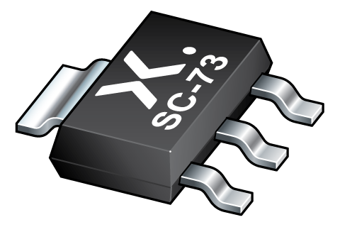
SC-73
5
EUROPEAN
PROJECTION
ISSUE DATE
97-02-28
99-09-13
�NXP Semiconductors
Product data sheet
Schottky barrier double diodes
BAT120 series
DATA SHEET STATUS
DOCUMENT
STATUS(1)
PRODUCT
STATUS(2)
DEFINITION
Objective data sheet
Development
This document contains data from the objective specification for product
development.
Preliminary data sheet
Qualification
This document contains data from the preliminary specification.
Product data sheet
Production
This document contains the product specification.
Notes
1. Please consult the most recently issued document before initiating or completing a design.
2. The product status of device(s) described in this document may have changed since this document was published
and may differ in case of multiple devices. The latest product status information is available on the Internet at
URL http://www.nxp.com.
DISCLAIMERS
above those given in the Characteristics sections of this
document is not implied. Exposure to limiting values for
extended periods may affect device reliability.
General ⎯ Information in this document is believed to be
accurate and reliable. However, NXP Semiconductors
does not give any representations or warranties,
expressed or implied, as to the accuracy or completeness
of such information and shall have no liability for the
consequences of use of such information.
Terms and conditions of sale ⎯ NXP Semiconductors
products are sold subject to the general terms and
conditions of commercial sale, as published at
http://www.nxp.com/profile/terms, including those
pertaining to warranty, intellectual property rights
infringement and limitation of liability, unless explicitly
otherwise agreed to in writing by NXP Semiconductors. In
case of any inconsistency or conflict between information
in this document and such terms and conditions, the latter
will prevail.
Right to make changes ⎯ NXP Semiconductors
reserves the right to make changes to information
published in this document, including without limitation
specifications and product descriptions, at any time and
without notice. This document supersedes and replaces all
information supplied prior to the publication hereof.
No offer to sell or license ⎯ Nothing in this document
may be interpreted or construed as an offer to sell products
that is open for acceptance or the grant, conveyance or
implication of any license under any copyrights, patents or
other industrial or intellectual property rights.
Suitability for use ⎯ NXP Semiconductors products are
not designed, authorized or warranted to be suitable for
use in medical, military, aircraft, space or life support
equipment, nor in applications where failure or malfunction
of an NXP Semiconductors product can reasonably be
expected to result in personal injury, death or severe
property or environmental damage. NXP Semiconductors
accepts no liability for inclusion and/or use of NXP
Semiconductors products in such equipment or
applications and therefore such inclusion and/or use is at
the customer’s own risk.
Export control ⎯ This document as well as the item(s)
described herein may be subject to export control
regulations. Export might require a prior authorization from
national authorities.
Quick reference data ⎯ The Quick reference data is an
extract of the product data given in the Limiting values and
Characteristics sections of this document, and as such is
not complete, exhaustive or legally binding.
Applications ⎯ Applications that are described herein for
any of these products are for illustrative purposes only.
NXP Semiconductors makes no representation or
warranty that such applications will be suitable for the
specified use without further testing or modification.
Limiting values ⎯ Stress above one or more limiting
values (as defined in the Absolute Maximum Ratings
System of IEC 60134) may cause permanent damage to
the device. Limiting values are stress ratings only and
operation of the device at these or any other conditions
2003 Aug 04
6
�NXP Semiconductors
Customer notification
This data sheet was changed to reflect the new company name NXP Semiconductors. No changes were
made to the content, except for the legal definitions and disclaimers.
Contact information
For additional information please visit: http://www.nxp.com
For sales offices addresses send e-mail to: salesaddresses@nxp.com
© NXP B.V. 2009
All rights are reserved. Reproduction in whole or in part is prohibited without the prior written consent of the copyright owner.
The information presented in this document does not form part of any quotation or contract, is believed to be accurate and reliable and may be changed
without notice. No liability will be accepted by the publisher for any consequence of its use. Publication thereof does not convey nor imply any license
under patent- or other industrial or intellectual property rights.
Printed in The Netherlands
613514/04/pp7
Date of release: 2003 Aug 04
Document order number: 9397 750 11054
�
很抱歉,暂时无法提供与“BAT120S,115”相匹配的价格&库存,您可以联系我们找货
免费人工找货