BZX100A
Single Zener diode
Rev. 01 — 30 May 2007
Product data sheet
1. Product profile
1.1 General description
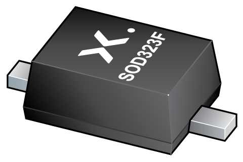
General-purpose Zener diode in a SOD323F (SC-90) very small and flat lead
Surface-Mounted Device (SMD) plastic package.
1.2 Features
n Non-repetitive peak reverse power dissipation: ≤ 60 W
n Small plastic package suitable for surface-mounted design
1.3 Applications
n General regulation functions
n Overvoltage protection for ElectroLuminescent (EL) driver circuits
n AEC-Q101 qualified
1.4 Quick reference data
Table 1.
Quick reference data
Symbol
Parameter
Conditions
Min
Typ
Max
Unit
VZ
working voltage
IZ = 1 mA
95
-
105
V
IZSM
non-repetitive peak reverse
current
-
-
0.5
A
[1]
[1]
tp = 100 µs; square wave; Tj = 25 °C prior to surge
2. Pinning information
Table 2.
Pin
Pinning
Description
1
cathode
2
anode
Simplified outline
Symbol
[1]
1
2
1
2
006aaa152
[1]
The marking bar indicates the cathode.
�BZX100A
Nexperia
Single Zener diode
3. Ordering information
Table 3.
Ordering information
Type number
BZX100A
Package
Name
Description
Version
SC-90
plastic surface-mounted package; 2 leads
SOD323F
4. Marking
Table 4.
Marking codes
Type number
Marking code
BZX100A
AS
5. Limiting values
Table 5.
Limiting values
In accordance with the Absolute Maximum Rating System (IEC 60134).
Symbol
Parameter
Conditions
IF
forward current
-
0.2
A
IZSM
non-repetitive peak reverse
current
[1]
-
0.5
A
PZSM
non-repetitive peak reverse
power dissipation
[1]
-
60
W
Ptot
total power dissipation
[2]
-
310
mW
[3]
-
550
mW
[4]
-
1
W
Tamb ≤ 25 °C
Max
Unit
Tj
junction temperature
-
150
°C
Tamb
ambient temperature
−65
+150
°C
Tstg
storage temperature
−65
+150
°C
[1]
tp = 100 µs; square wave; Tj = 25 °C prior to surge
[2]
Device mounted on an FR4 Printed-Circuit Board (PCB), single-sided copper, tin-plated and standard
footprint.
[3]
Device mounted on an FR4 PCB, single-sided copper, tin-plated, mounting pad for cathode 1 cm2.
[4]
Device mounted on a ceramic PCB, Al2O3, standard footprint.
BZX100A
Product data sheet
Min
© Nexperia B.V. 2007. All rights reserved.
Rev. 01 — 30 May 2007
2 of 10
�BZX100A
Nexperia
Single Zener diode
006aab047
1.2
(1)
Ptot
(W)
0.8
(2)
0.4
0
−75
(3)
−25
25
75
125
175
Tamb (°C)
(1) Ceramic PCB, Al2O3, standard footprint
(2) FR4 PCB, mounting pad for cathode 1 cm2
(3) FR4 PCB, standard footprint
Fig 1. Power derating curves
6. Thermal characteristics
Table 6.
Symbol
Rth(j-a)
Rth(j-sp)
Thermal characteristics
Parameter
Conditions
thermal resistance from
junction to ambient
in free air
thermal resistance from
junction to solder point
Typ
Max
Unit
-
-
400
K/W
[2]
-
-
230
K/W
[3]
-
-
125
K/W
[4]
-
-
55
K/W
[1]
Device mounted on an FR4 PCB, single-sided copper, tin-plated and standard footprint.
[2]
Device mounted on an FR4 PCB, single-sided copper, tin-plated, mounting pad for cathode 1 cm2.
[3]
Device mounted on a ceramic PCB, Al2O3, standard footprint.
[4]
Soldering point of cathode tab.
BZX100A
Product data sheet
Min
[1]
© Nexperia B.V. 2007. All rights reserved.
Rev. 01 — 30 May 2007
3 of 10
�BZX100A
Nexperia
Single Zener diode
7. Characteristics
Table 7.
Characteristics
Tj = 25 °C unless otherwise specified.
Symbol
Parameter
Conditions
Min
Typ
Max
Unit
IF = 10 mA
-
-
0.9
V
IF = 100 mA
-
-
1.1
V
[1]
forward voltage
VF
VZ
working voltage
IZ = 1 mA
95
-
105
V
rdif
differential resistance
IZ = 1 mA
-
-
700
Ω
IR
reverse current
VR = 76 V
-
-
0.2
µA
SZ
temperature coefficient
IZ = 1 mA
-
138
-
mV/K
Cd
diode capacitance
f = 1 MHz;
VR = 0 V
-
-
70
pF
[1]
Pulse test: tp ≤ 300 µs; δ ≤ 0.02.
006aab048
103
006aab049
300
PZSM
(W)
IF
(mA)
102
200
10
100
1
10−5
10−4
10−3
10−2
0
0.6
tp (s)
0.8
0.9
1.0
VF (V)
Tj = 25 °C (prior to surge)
Tj = 25 °C
Fig 2. Non-repetitive peak reverse power dissipation
as a function of pulse duration; maximum
values
Fig 3. Forward current as a function of forward
voltage; typical values
BZX100A
Product data sheet
0.7
© Nexperia B.V. 2007. All rights reserved.
Rev. 01 — 30 May 2007
4 of 10
�BZX100A
Nexperia
Single Zener diode
006aab050
150
006aab051
10−3
IZ
(A)
10−4
SZ
(mV/K)
140
10−5
130
10−6
120
10−7
110
10−8
10−9
100
0
1
2
3
4
5
80
90
100
110
IZ (mA)
120
VZ (V)
Tj = 25 °C to 150 °C
Tj = 25 °C
Fig 4. Temperature coefficient as a function of
working current; typical values
Fig 5. Working current as a function of working
voltage; typical values
8. Application information
High-voltage Zener diodes can be used as overvoltage protection diodes for Integrated
Circuits (IC) due to their ability to cut off the applied voltage at a well-defined value. One
important application is the protection of EL driver circuits where a driver IC is connected
to an EL foil. Since both the foil as well as the IC are sensitive against voltage overstress,
it is necessary to install an additional protection device in the circuit. Commonly, a
peak-to-peak voltage of 220 V should not be exceeded, such that two 100 V diodes in
back-to-back configuration are used.
CHF
CHF
CLF
CLF
Renable
ENABLE
E
n.c.
GND
1
10
2
9
3
DRIVER IC
8
4
7
5
6
V+
VBAT
L+
VO
L
L−
n.c.
BZX100A
BZX100A
EL LAMP
006aab052
Fig 6. Application diagram
BZX100A
Product data sheet
© Nexperia B.V. 2007. All rights reserved.
Rev. 01 — 30 May 2007
5 of 10
�BZX100A
Nexperia
Single Zener diode
9. Test information
9.1 Quality information
This product has been qualified in accordance with the Automotive Electronics Council
(AEC) standard Q101 (Stress qualification for discrete semiconductors) and is suitable for
use in automotive critical applications.
10. Package outline
1.35
1.15
0.80
0.65
0.5
0.3
1
2.7
2.3
1.8
1.6
2
0.40
0.25
Dimensions in mm
0.25
0.10
04-09-13
Fig 7. Package outline SOD323F (SC-90)
11. Packing information
Please refer to packing information on www.nexperia.com.
BZX100A
Product data sheet
© Nexperia B.V. 2007. All rights reserved.
Rev. 01 — 30 May 2007
6 of 10
�BZX100A
Nexperia
Single Zener diode
12. Soldering
3.05
2.80
2.10
1.60
solder lands
solder resist
1.65
0.95
0.50
0.60
occupied area
solder paste
0.50
(2×)
msa433
Reflow soldering is the only recommended soldering method.
Dimensions in mm
Fig 8. Reflow soldering footprint SOD323F (SC-90)
BZX100A
Product data sheet
© Nexperia B.V. 2007. All rights reserved.
Rev. 01 — 30 May 2007
7 of 10
�BZX100A
Nexperia
Single Zener diode
13. Revision history
Table 9.
Revision history
Document ID
Release date
Data sheet status
Change notice
Supersedes
BZX100A
20070530
Product data sheet
-
-
BZX100A
Product data sheet
© Nexperia B.V. 2007. All rights reserved.
Rev. 01 — 30 May 2007
8 of 10
�BZX100A
Nexperia
Single Zener diode
14. Legal information
14.1 Data sheet status
Document status[1][2]
Product status[3]
Definition
Objective [short] data sheet
Development
This document contains data from the objective specification for product development.
Preliminary [short] data sheet
Qualification
This document contains data from the preliminary specification.
Product [short] data sheet
Production
This document contains the product specification.
[1]
Please consult the most recently issued document before initiating or completing a design.
[2]
The term ‘short data sheet’ is explained in section “Definitions”.
[3]
The product status of device(s) described in this document may have changed since this document was published and may differ in case of multiple devices. The latest product status
information is available on the Internet at URL http://www.nexperia.com.
14.2 Definitions
Draft — The document is a draft version only. The content is still under
internal review and subject to formal approval, which may result in
modifications or additions. Nexperia does not give any representations or
warranties as to the accuracy or completeness of information included herein
and shall have no liability for the consequences of use of such information.
Short data sheet — A short data sheet is an extract from a full data sheet
with the same product type number(s) and title. A short data sheet is
intended for quick reference only and should not be relied upon to contain
detailed and full information. For detailed and full information see the
relevant full data sheet, which is available on request via the local Nexperia
sales office. In case of any inconsistency or conflict with the short data sheet,
the full data sheet shall prevail.
14.3 Disclaimers
General — Information in this document is believed to be accurate and
reliable. However, Nexperia does not give any representations or warranties,
expressed or implied, as to the accuracy or completeness of such information
and shall have no liability for the consequences of use of such information.
malfunction of a Nexperia product can reasonably be expected to result in
personal injury, death or severe property or environmental damage. Nexperia
accepts no liability for inclusion and/or use of Nexperia products in such
equipment or applications and therefore such inclusion and/or use is at the
customer’s own risk.
Applications — Applications that are described herein for any of these
products are for illustrative purposes only. Nexperia makes no representation
or warranty that such applications will be suitable for the specified use
without further testing or modification.
Limiting values — Stress above one or more limiting values (as defined in
the Absolute Maximum Ratings System of IEC 60134) may cause permanent
damage to the device. Limiting values are stress ratings only and operation of
the device at these or any other conditions above those given in the
Characteristics sections of this document is not implied. Exposure to limiting
values for extended periods may affect device reliability.
Terms and conditions of sale — Nexperia products are sold subject to the
general terms and conditions of commercial sale, as published at http://
www.nexperia.com/profile/terms, including those pertaining to warranty,
intellectual property rights infringement and limitation of liability, unless
explicitly otherwise agreed to in writing by Nexperia. In case of any
inconsistency or conflict between information in this document and such
terms and conditions, the latter will prevail.
Right to make changes — Nexperia reserves the right to make changes to
information published in this document, including without limitation
specifications and product descriptions, at any time and without notice. This
document supersedes and replaces all information supplied prior to the
publication hereof.
No offer to sell or license — Nothing in this document may be interpreted
or construed as an offer to sell products that is open for acceptance or the
grant, conveyance or implication of any license under any copyrights, patents
or other industrial or intellectual property rights.
Suitability for use — Nexperia products are not designed, authorized or
warranted to be suitable for use in medical, military, aircraft, space or life
support equipment, nor in applications where failure or
14.4 Trademarks
Notice: All referenced brands, product names, service names and trademarks
are the property of their respective owners.
BZX100A
Product data sheet
© Nexperia B.V. 2007. All rights reserved.
Rev. 01 — 30 May 2007
9 of 10
�BZX100A
Nexperia
Single Zener diode
15. Contents
1
1.1
1.2
1.3
1.4
2
3
4
5
6
7
8
9
9.1
10
11
12
13
14
14.1
14.2
14.3
14.4
15
Product profile . . . . . . . . . . . . . . . . . . . . . . . . . .
General description. . . . . . . . . . . . . . . . . . . . . .
Features . . . . . . . . . . . . . . . . . . . . . . . . . . . . . .
Applications . . . . . . . . . . . . . . . . . . . . . . . . . . .
Quick reference data. . . . . . . . . . . . . . . . . . . . .
Pinning information . . . . . . . . . . . . . . . . . . . . . .
Ordering information . . . . . . . . . . . . . . . . . . . . .
Marking . . . . . . . . . . . . . . . . . . . . . . . . . . . . . . . .
Limiting values. . . . . . . . . . . . . . . . . . . . . . . . . .
Thermal characteristics. . . . . . . . . . . . . . . . . . .
Characteristics . . . . . . . . . . . . . . . . . . . . . . . . . .
Application information. . . . . . . . . . . . . . . . . . .
Test information . . . . . . . . . . . . . . . . . . . . . . . . .
Quality information . . . . . . . . . . . . . . . . . . . . . .
Package outline . . . . . . . . . . . . . . . . . . . . . . . . .
Packing information. . . . . . . . . . . . . . . . . . . . . .
Soldering . . . . . . . . . . . . . . . . . . . . . . . . . . . . . .
Revision history . . . . . . . . . . . . . . . . . . . . . . . . .
Legal information. . . . . . . . . . . . . . . . . . . . . . . .
Data sheet status . . . . . . . . . . . . . . . . . . . . . . .
Definitions . . . . . . . . . . . . . . . . . . . . . . . . . . . . .
Disclaimers . . . . . . . . . . . . . . . . . . . . . . . . . . . .
Trademarks . . . . . . . . . . . . . . . . . . . . . . . . . . . .
1
1
1
1
1
1
2
2
2
3
4
5
6
6
6
6
7
8
9
9
9
9
9
Contents . . . . . . . . . . . . . . . . . . . . . . . . . . . . . . 10
Please be aware that important notices concerning this document and the product(s)
described herein, have been included in section ‘Legal information’.
© Nexperia B.V. 2007.
All rights reserved.
For more information, please visit: http://www.nexperia.com
For sales office addresses, please send an email to:
salesaddresses@nexperia.com
Date of release: 30 May 2007
Document identifier: BZX100A
�