Product Specification
RoHS compliant & Halogen Free
Surface-mount Ceramic Multilayer Capacitors
Part Description :
X7R/2220/1.0uF/50V/±10%
Yageo Part number : CC2220KKX7R9BB105
Page.1
�SCOPE
This product specification is applied to Multi-layer Ceramic Capacitor used for
General Electronic equipment.
Description
The capacitor consists of a rectangular block of ceramic dielectric in which a number of
interleaved nickel electrodes are contained. This structure gives rise to a high capacitance
per unit volume.
The inner electrodes are connected to the two end terminations and finally covered with
a layer of plated tin (NiSn).The terminations are lead-free. A cross section of the structure
is shown in Fig.1.
MECHANICAL DATA
Fig. 2 Component outline
Physical dimensions (all in mm)
Size
L1
2220
5.7 ±0.40
W
T
5.0 ±0.30 1.15±0.1
L2/L3
Max
Min
0.25
0.75
L4
Min
3.40
Thickness classification and packaging quantities:
Thickness Classification
1.15±0.1 mm
Tape Width
Embossed plastic tape reel 7"
Amount
1,500
Page.2
�ELECTRICAL CHARACTERISTICS
Unless otherwise specified, all test and measurements shall be made under standard
atmospheric conditions for testing as given in 5.3 of IEC 60068-1:
--temperature: 15℃ to 35℃
--relative humidity: 25% to 75%
--air pressure: 86 kPa to 106 kPa
Before the measurements are made, the capacitor shall be stored at the measuring
temperature for a time sufficient to allow the entire capacitor to reach this temperature.
The period as prescribed for recovery at the end of a test is normally sufficient for this purpose.
Capacitance range
Temperature range
Tolerance on capacitance after 1000 hours
Rated voltage UR(DC)
Tan δ
Insulation resistance after 1 minute at U R (DC)
Maximum capacitance change as
a function of temperature
Terminations
Resistance to soldering heat
1.0uF
-55°C to +125°C
±10%
50V
≦2.5%
Rins. ≧ 10GOhm or Rins. x C≧ 500 s whichever is less.
±15%
Ni/Sn Barrier
260°C, 10 sec
STORAGE CONDITIONS
The products must be stored and shipping in an ambient temperature of less than 40°C
with a relative humidity of less than 70%.
Page.3
�METHOD OF MOUNTING
For normal use the capacitors may be mounted on printed-circuit boards or ceramic substrates
by applying wave soldering, reflow soldering or conductive adhesive in accordance
with “IEC 61760-1” (Standard method for the specification of surface mounting components).
Page.4
�SOLDERING RECOMMENDATION
Soldering Method
Reflow
Reflow / Wave
Size
0402
0603
≧ 0.1 uF
≧ 1.0 uF
≧ 2.2 uF ≧ 4.7 uF Reflow only
< 0.1 uF
< 1.0 uF
< 2.2 uF
0805
1206
≧ 1210
< 4.7 uF ----
Page.5
�Test procedures and requirements.
TEST
PROCEDURE
REQUIREMENTS
Mounting
The capacitors may be mounted on printed-circuit boards or
ceramic substrates
No visible damage
Visual inspection and Any applicable method using x10 magnification
dimension check
In accordance with specification
Capacitance
Within specified tolerance
Class1:
C ≤1nF, f = 1 MHz;
C >1nF, f = 1 KHz;
NP0: measuring voltage 1 V at 20℃
Class 2:
Precondition:
150 +0/-10 ℃/1 hr , then keep for 24±1 hrs at room temp
C ≤10uF, f = 1 KHz; measuring voltage 1 V at 20℃
C >10uF, f = 120Hz; measuring voltage 0.5V at 20℃
Dissipation Factor
(D.F.)
Class1:
C ≤ 1nF, f = 1 MHz;
C >1nF, f = 1 KHz;
NP0: measuring voltage 1 V at 20 ℃
In accordance with specification
Class 2:
Precondition:
150 +0/-10 ℃/1 hr , then keep for 24±1 hrs at room temp
C ≤ 10uF, f = 1 KHz; measuring voltage 1 V at 20℃
C >10uF, f = 120Hz; measuring voltage 0.5V at 20℃
Insulation resistance At Ur (DC) for 1 minute
Voltage proof
In accordance with specification
No breakdown or flashover
Specified stress voltage applied for 1~5 seconds
Ur≤100V: series applied 2.5Ur
1001206:100 to 120 °C for 1 minute and 170 to
200°C for 1 minute.
Solder bath temperature: 260 ± 5°C;
Dipping time 10±0.5 s
Recovery time 24±2 Hours.
REQUIREMENTS
Dissolution of the end face plating shall not
exceed 25% of the length of the edge
concerned.
ΔC/C:
Class1:
NP0: within ±0.5% or 0.5 pF whichever is greater
Class2:
X7R/X5R: ±10%
Y5V: ±20%
D.F.:
within initial specified value
Solderability
Rapid change of
temperature
Rins:
within initial specified value
The specimen shall be preheated to a temperature of (80 to 140) The solder should cover over 95% of the critical
℃ and maintained for 30s to 60s.
area of each termination.
1. Temperature: 235±5°C / Dipping time: 2 ±0.5 s
2. Temperature: 245±5°C / Dipping time: 3 ±0.5 s (lead free)
Depth of immersion: 10mm
Preconditioning;
150 +0/-10℃/1 hr, then keep for24±1 hrs at room temp
5 cycles with following detail:
30 minutes at Lower Category Temperature;
30 minutes at Upper Category Temperature;
Recovery time 24±2 Hours.
No visual damage
ΔC/C:
Class1:
NP0:within 1% or 1 pF, whichever is greater
Class2:
X7R/X5R:±15%
Y5V:±20%
D.F.:
meet initial specified value
Rins:
meet initial specified value
�Test procedures and requirements.
TEST
PROCEDURE
REQUIREMENTS
Damp heat, with Ur
load
1. Preconditioning, class 2 only:
150 +0/-10℃ /1 hr , then keep for 24±1hrs
at room temp
No visual damage after recovery
2. Initial measure
Spec: refer Initial spec (C, D, IR)
3. Damp heat test:
500±12 hours at 40±2°C; 90 to 95% R.H.; 1.0Ur applied.
4. Recovery.
Class 1:6 to 24 hours
Class 2:24±2 hours
5. Final measure:
C, D, IR
P.S. If the capacitance value is less than the minimum value
permitted, then after the other measurements have been made
the capacitor shall be precondition according to IEC 60384 4.1
and then the requirement shall be met.
Endurance
1. Precondition, class 2 only:
150 +0/-10 ℃/1 hr , then keep for 24±1 hrs at room temp
2. Initial measure
Spec: refer Initial spec
C, D, IR
3. Endurance test:
Temperature:
NP0/X7R: 125℃
X5R/Y5V:85 ℃
Specified stress voltage applied for 1000 hrs
Applied 2.0 x Ur for general product.
ΔC/C:
NP0:within ±2% or 1 pF, whichever is greater
X7R/X5R:±15%
Y5V:±30%
D.F.:
NP0:2 × specified value
X7R/X5R:
≦16V:≦7%
≧25V:≦5%
Y5V:≦15%
Rins:
NP0:
≧2,500MΩ or RxC≧25s whichever is less
X7R/X5R/Y5V:
≧500MΩ or RxC≧25s whichever is less
No visual damage
ΔC/C:
NP0:within ±2% or 1 pF, whichever is greater
X7R/X5R:± 15%
Y5V:± 30%
D.F.:
NP0:2 × specified value
X7R/X5R:
≦16V:≦7%
≧25V:≦5%
Y5V:≦15%
4. Recovery time: 24±2 hours
Rins:
NP0:
≧4,000MΩ or RxC≧40s whichever is less
P.S. If the capacitance value is less than the minimum value
X7R/Y5V/X5R:
permitted, then after the other measurements have been made
the capacitor shall be precondition according to IEC 60384 4.1 ≧1000MΩ or RxC≧50s whichever is less
and then the requirement shall be met.
5. Final measure: C ,D, IR
�
很抱歉,暂时无法提供与“CC2220KKX7R9BB105”相匹配的价格&库存,您可以联系我们找货
免费人工找货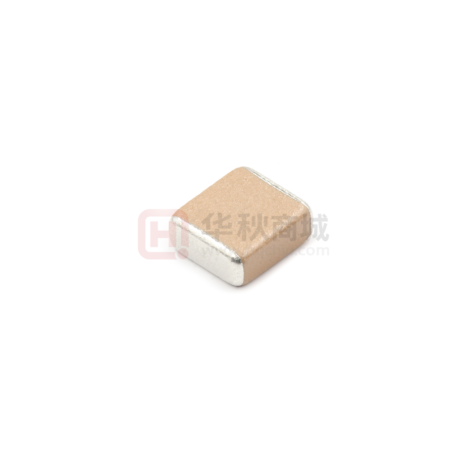


 工商网监
湘ICP备2023018690号
工商网监
湘ICP备2023018690号