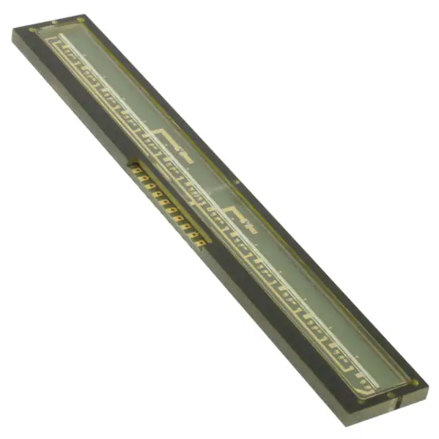
TSL2014
896 y 1 LINEAR SENSOR ARRAY
r
r
D
D
D
D
D
D
D
D
D
TAOS040C − AUGUST 2011
896 × 1 Sensor-Element Organization
200 Dots-Per-Inch (DPI) Sensor Pitch
High Linearity and Uniformity
Wide Dynamic Range . . . 2000:1 (66 dB)
Output Referenced to Ground
Low Image Lag . . . 0.5% Typ
Operation to 5 MHz
Single 5-V Supply
112 mm Active Length
PACKAGE
(TOP VIEW)
VDD 1
SI1 2
AO1 3
SO1 4
SI2 5
CLK 6
GND 7
AO2 8
SO2 9
VDD 10
Description
The TSL2014 linear sensor array consists of two
sections of 448 photodiodes and associated charge
amplifier circuitry that can be connected to form a
contiguous 896 × 1 array. The pixels measure 120 μm
(H) by 70 μm (W) with 125-μm center-to-center spacing
and 55-μm spacing between pixels. Operation is
simplified by internal control logic that requires only a
serial-input (SI) signal and a clock.
The TSL2014 is intended for use in a wide variety of
applications including mark detection and code
reading, optical character recognition (OCR) and
contact imaging, edge detection and positioning as well
as optical linear and rotary encoding.
Functional Block Diagram (each section)
Pixel 1
(449)
S1
_
+
Pixel
2
(450)
1 Integrator
Reset
2
Pixel
3
(451)
VDD
Analog
Bus
2
1
Pixel
448
(896)
3
Output
Amplifier
AO1
(AO2)
S2
Sample/
Output
RL
External
Load
Gain Trim
Switch Control Logic
SO1
(SO2)
Q1
CLK
Q2
Q3
Q448 (896)
448-Bit Shift Register
SI1 (SI2)
The LUMENOLOGY r Company
Copyright E 2011, TAOS Inc.
r
Texas Advanced Optoelectronic Solutions Inc.
1001 Klein Road S Suite 300 S Plano, TX 75074 S (972)
r 673-0759
www.taosinc.com
1
�TSL2014
896 y 1 LINEAR SENSOR ARRAY
TAOS040C − AUGUST 2011
Terminal Functions
TERMINAL
NAME
NO.
I/O
DESCRIPTION
AO1
3
O
Analog output of section 1.
AO2
8
O
Analog output of section 2.
CLK
6
I
Clock. The clock controls the charge transfer, pixel output and reset.
GND
7
SI1
2
I
Serial input (section 1). SI1 defines the start of the data-out sequence.
SI2
5
I
Serial input (section 2). SI2 defines the start of the data-out sequence.
SO1
4
O
Serial output (section 1). SO1 signals the end of the data out sequence and provides a signal to drive the input
of section 2 (SI2) in serial mode.
SO2
9
O
Serial output (section 2). SO2 signals the end of the data out sequence and provides a signal to drive the input
of another device for cascading.
VDD
1, 10
Ground (substrate). All voltages are referenced to GND.
Supply voltage. Supply voltage for both analog and digital circuits.
Detailed Description
The sensor consists of 896 photodiodes arranged in a linear array. Light energy impinging on a photodiode
generates photocurrent, which is integrated by the active integration circuitry associated with that pixel. During
the integration period, a sampling capacitor connects to the output of the integrator through an analog switch.
The amount of charge accumulated at each pixel is directly proportional to the light intensity and the integration
time. The integration time is the interval between two consecutive output periods.
The output and reset of the integrators is controlled by two 448-bit shift registers and reset logic. A 448-pixel
output cycle is initiated by clocking in a logic 1 into the SI input of a section for one positive going clock edge
(see Figures1 and 2) †. The two 448-pixel sections may be operated independently using a single clock input
or connected in series to form a 896-pixel array. Each section has an independent output (AO), which may be
connected together for the 896-pixel function.
When operating in the 896-pixel mode, as the SI pulse is clocked through the 896-bit shift register, the charge
on the sampling capacitor of each pixel is sequentially connected to a charge-coupled output amplifier that
generates a voltage output, AO. When the bit position goes low, the pixel integrator is reset. On the 897th clock
rising edge, the SI pulse is clocked out of the shift register (S2) and the output assumes a high-impedance state.
Note that this 897th clock pulse is required to terminate the output of the 896th pixel and return the internal logic
to a known state. A subsequent SI pulse can be presented as early as the 898th clock pulse, thereby initiating
another pixel output cycle.
The voltage developed at analog output (AO) is given by:
Vout = Vdrk + (Re) (Ee) (tint)
where:
Vout
Vdrk
Re
Ee
tint
is the analog output voltage for white condition
is the analog output voltage for dark condition
is the device responsivity for a given wavelength of light given in V/(μJ/cm2)
is the incident irradiance in μW/cm2
is integration time in seconds
AO is driven by a source follower that requires an external pulldown resistor (330-Ω typical). The output is
nominally 0 V for no light input, 2 V for normal white-level, and 3.4 V for saturation light level. When the device
is not in the output phase, AO is in a high impedance state.
A 0.1 μF bypass capacitor should be connected between VDD and ground as close as possible to the device.
†
For proper operation, after meeting the minimum hold time condition, SI must go low before the next rising edge of the clock.
Copyright E 2011, TAOS Inc.
The LUMENOLOGY r Company
r
r
2
www.taosinc.com
�TSL2014
896 y 1 LINEAR SENSOR ARRAY
TAOS040C − AUGUST 2011
Absolute Maximum Ratings†
Supply voltage range, VDD . . . . . . . . . . . . . . . . . . . . . . . . . . . . . . . . . . . . . . . . . . . . . . . . . . . . . . . . . . . −0.3 V to 6 V
Input voltage range, VI . . . . . . . . . . . . . . . . . . . . . . . . . . . . . . . . . . . . . . . . . . . . . . . . . . . . . . −0.3 V to VDD + 0.3V
Input clamp current, IIK (VI < 0 or VI > VDD) . . . . . . . . . . . . . . . . . . . . . . . . . . . . . . . . . . . . . . . . −20 mA to 20 mA
Output clamp current, IOK (VO < 0 or VO > VDD) . . . . . . . . . . . . . . . . . . . . . . . . . . . . . . . . . . . . −25 mA to 25 mA
Voltage range applied to any output in the high impedance or
power-off state, VO . . . . . . . . . . . . . . . . . . . . . . . . . . . . . . . . . . . . . . . . . . . . . . . . . . . −0.3 V to VDD + 0.3V
Continuous output current, IO (VO = 0 to VDD) . . . . . . . . . . . . . . . . . . . . . . . . . . . . . . . . . . . . . . −25 mA to 25 mA
Continuous current through VDD or GND . . . . . . . . . . . . . . . . . . . . . . . . . . . . . . . . . . . . . . . −150 mA to 150 mA
Analog output current range, IO . . . . . . . . . . . . . . . . . . . . . . . . . . . . . . . . . . . . . . . . . . . . . . . . . . −25 mA to 25 mA
Operating free-air temperature range, TA . . . . . . . . . . . . . . . . . . . . . . . . . . . . . . . . . . . . . . . . . . . . −25°C to 85°C
Storage temperature range, Tstg . . . . . . . . . . . . . . . . . . . . . . . . . . . . . . . . . . . . . . . . . . . . . . . . . . . . −25°C to 85°C
Lead temperature on solder pads for 10 seconds . . . . . . . . . . . . . . . . . . . . . . . . . . . . . . . . . . . . . . . . . . . . 260°C
ESD tolerance, human body model . . . . . . . . . . . . . . . . . . . . . . . . . . . . . . . . . . . . . . . . . . . . . . . . . . . . . . . . 2000 V
†
Stresses beyond those listed under “Absolute Maximum Ratings” may cause permanent damage to the device. These are stress ratings only, and
functional operation of the device at these or any other conditions beyond those indicated under “Recommended Operating Conditions” is not
implied. Exposure to absolute-maximum-rated conditions for extended periods may affect device reliability.
Recommended Operating Conditions (see Figure 1 and Figure 2)
Supply voltage, VDD
MIN
NOM
4.5
5
MAX
UNIT
5.5
V
Input voltage, VI
0
VDD
V
High-level input voltage, VIH
Low-level input voltage, VIL
2
VDD
V
Wavelength of light source, λ
Clock frequency, fclock
Sensor integration time, serial tint
Sensor integration time, parallel tint
Operating free-air temperature, TA
Load resistance, RL
Load capacitance, CL
The LUMENOLOGY r Company
0
0.8
400
1000
nm
V
5
5000
kHz
0.1792
100
ms
0.090
100
ms
0
70
°C
300
4700
Ω
330
pF
Copyright E 2011, TAOS Inc.
r
r
www.taosinc.com
3
�TSL2014
896 y 1 LINEAR SENSOR ARRAY
TAOS040C − AUGUST 2011
Electrical Characteristics at fclock = 200 kHz, VDD = 5 V, TA = 25°C, λp = 640 nm, tint = 5 ms,
RL = 330 Ω, Ee = 18μW/cm2 (unless otherwise noted)
PARAMETER
TEST CONDITIONS
See Note 1
MIN
TYP
MAX
1.6
2
2.4
V
0
0.05
0.15
V
7%
20%
Vout
Analog output voltage (white, average over 896 pixels)
Vdrk
Analog output voltage (dark, average over 896 pixels)
PRNU
Pixel response nonuniformity
See Notes 2 & 3
Nonlinearity of analog output voltage
See Note 3
± 0.4%
Output noise voltage
See Note 4
1
Re
Responsivity
16
SE
Saturation exposure
Vsat
Analog output saturation voltage
DSNU
Dark signal nonuniformity
All pixels
IL
Image lag
See Note 7
IDD
Supply current, output idle
IIH
High-level input current
VI = VDD
IIL
Low-level input current
VI = 0
See Note 5
22
FS
mVrms
28
2.5
3.4
25
V/
(μJ/cm 2)
nJ/cm 2
155
See Note 6
UNIT
V
120
mV
80
mA
10
μA
10
μA
0.5%
53
IO = 50 μA
4.5
4.95
VOH
High level output voltage,
High-level
voltage SO1 and SO2
VOL
Low level output voltage,
Low-level
voltage SO1 and SO2
Ci(SI)
Input capacitance, SI
35
pF
Ci(CLK)
Input capacitance, CLK
70
pF
IO = 4 mA
4.6
IO = 50 μA
0.01
IO = 4 mA
0.4
V
0.1
V
NOTES: 1. The array is uniformly illuminated with a diffused LED source having a peak wavelength of 640 nm.
2. PRNU is the maximum difference between the voltage from any single pixel and the average output voltage from all pixels of the
device under test when the array is uniformly illuminated at the white irradiance level. PRNU includes DSNU.
3. Nonlinearity is defined as the maximum deviation from a best-fit straight line over the dark-to-white irradiance levels, as a percent
of analog output voltage (white).
4. RMS noise is the standard deviation of a single-pixel output under constant illumination as observed over a 5-second period.
5. Minimum saturation exposure is calculated using the minimum Vsat, the maximum Vdrk, and the maximum Re.
6. DSNU is the difference between the maximum and minimum output voltage in the absence of illumination.
7. Image lag is a residual signal left in a pixel from a previous exposure. It is defined as a percent of white-level signal remaining after
a pixel is exposed to a white condition followed by a dark condition:
IL +
V out (IL) * V drk
V out (white) * V drk
100
Timing Requirements (see Figure 1 and Figure 2)
MIN
tsu(SI)
Setup time, serial input (see Note 8)
th(SI)
Hold time, serial input (see Note 8 and Note 9)
tw
Pulse duration, clock high or low
50
tr, tf
Input transition (rise and fall) time
0
NOM
MAX
UNIT
20
ns
0
ns
ns
500
ns
NOTES: 8. Input pulses have the following characteristics: tr = 6 ns, tf = 6 ns.
9. SI must go low before the rising edge of the next clock pulse.
Copyright E 2011, TAOS Inc.
The LUMENOLOGY r Company
r
r
4
www.taosinc.com
�TSL2014
896 y 1 LINEAR SENSOR ARRAY
TAOS040C − AUGUST 2011
Dynamic Characteristics over recommended ranges of supply voltage and operating free-air
temperature (see Figure 2)
PARAMETER
TEST CONDITIONS
ts
Analog output settling time to ± 1%
RL = 330 Ω
tpd
Propagation delay time, SO1 and SO2
MIN
CL = 10 pF
TYP
MAX
UNIT
185
ns
50
ns
TYPICAL CHARACTERISTICS
CLK
SI
ÎÎÎÎÎÎÎÎÎÎÎÎÎÎÎÎÎÎÎÎ
ÎÎÎÎÎÎÎÎ
ÎÎÎÎÎÎÎÎÎÎÎÎÎÎÎÎÎÎÎÎÎÎÎÎÎÎÎÎ
449 Clock Cycles
AO
Hi-Z
Hi-Z
Figure 1. Timing Waveforms (each section)
tw
1 (449)
2 (450)
448 (896)
449 (897)
5V
CLK
2.5 V
2.5 V
2.5 V
0V
tsu(SI)
5V
SI1 (SI2) 2.5 V
2.5 V
0V
th(SI)
tpd(SO)
tpd(SO)
SO1 (SO2)
ts
ts
AO1 (A02)
Pixel 1 (449)
Pixel 448 (896)
Figure 2. Operational Waveforms (each section)
The LUMENOLOGY r Company
Copyright E 2011, TAOS Inc.
r
r
www.taosinc.com
5
�TSL2014
896 y 1 LINEAR SENSOR ARRAY
TAOS040C − AUGUST 2011
TYPICAL CHARACTERISTICS
ANALOG OUTPUT SETTLING TIME
vs
LOAD CAPACITANCE AND RESISTANCE
PHOTODIODE SPECTRAL RESPONSIVITY
1
600
TA = 25°C
500
ts — Settling Time to 1% — ns
0.8
Normalized Responsivity
470 pF
VDD = 5 V
Vout = 1 V
0.6
0.4
0.2
220 pF
400
100 pF
300
10 pF
200
100
0
300
400
500
600
700
800
900
1000 1100
λ − Wavelength − nm
0
0
200
400
Figure 3
Copyright E 2011, TAOS Inc.
800
1000
1200
Figure 4
The LUMENOLOGY r Company
r
r
6
600
RL − Load Resistance − Ω
www.taosinc.com
�TSL2014
896 y 1 LINEAR SENSOR ARRAY
TAOS040C − AUGUST 2011
APPLICATION INFORMATION
Integration Time
The integration time of the linear array is the period during which light is sampled and charge accumulates on
each pixel’s integrating capacitor. The flexibility to adjust the integration period is a powerful and useful feature
of the TAOS TSL2xx linear array family. By changing the integration time, a desired output voltage can be
obtained on the output pin while avoiding saturation for a wide range of light levels.
Each pixel of the linear array consists of a light-sensitive photodiode. The photodiode converts light intensity
to a voltage. The voltage is sampled on the Sampling Capacitor by closing switch S2 (position 1) (see the
functional block diagram on page 1). Logic controls the resetting of the Integrating Capacitor to zero by closing
switch S1 (position 2).
At SI input (Start Integration), pixel 1 is accessed. During this event, S2 moves from position 1 (sampling) to
position 3 (holding). This holds the sampled voltage for pixel 1. Switch S1 for pixel 1 is then moved to position
2. This resets (clears) the voltage previously integrated for that pixel so that pixel 1 is now ready to start a new
integration cycle. When the next clock period starts, the S1 switch is returned to position 1 to be ready to
start integrating again. S2 is returned to position 1 to start sampling the next light integration. Then the next pixel
starts the same procedure. The integration time is the time from a specific pixel read to the next time that pixel
is read again. If either the clock speed or the time between successive SI pulses is changed, the integration time
will vary. After the final (nth) pixel in the array is read on the output, the output goes into a high-impedance mode.
A new SI pulse can occur on the (n+1) clock causing a new cycle of integration/output to begin. Note that the
time between successive SI pulses must not exceed the maximum integration time of 100 msec.
The minimum integration time for any given array is determined by time required to clock out all the pixels in
the array and the time to discharge the pixels. The time required to discharge the pixels is a constant. Therefore,
the minimum integration period is simply a function of the clock frequency and the number of pixels in the array.
A slower clock speed increases the minimum integration time and reduces the maximum light level for saturation
on the output. The minimum integration time shown in this data sheet is based on the maximum clock frequency
of 5 MHz.
The minimum integration time can be calculated from the equation:
T int(min) +
1
ǒmaximum clock
Ǔ
frequency
n
where:
n
is the number of pixels
In the case of the TSL2014, the minimum integration time would be:
T int(min) + 200� ns
896 + 179.2� ms
It is important to note that not all pixels will have the same integration time if the clock frequency is varied while
data is being output.
The LUMENOLOGY r Company
Copyright E 2011, TAOS Inc.
r
r
www.taosinc.com
7
�TSL2014
896 y 1 LINEAR SENSOR ARRAY
TAOS040C − AUGUST 2011
APPLICATION INFORMATION
It is good practice on initial power up to run the clock (n+1) times after the first SI pulse to clock out indeterminate
data from power up. After that, the SI pulse is valid from the time following (n+1) clocks. The output will go into
a high-impedance state after the n+1 high clock edge. It is good practice to leave the clock in a low state when
inactive because the SI pulse required to start a new cycle is a low-to-high transition.
The integration time chosen is valid as long as it falls in the range between the minimum and maximum limits
for integration time. If the amount of light incident on the array during a given integration period produces a
saturated output (Max Voltage output), then the data is not accurate. If this occurs, the integration period should
be reduced until the analog output voltage for each pixel falls below the saturation level. The goal of reducing
the period of time the light sampling window is active is to lower the output voltage level to prevent saturation.
However, the integration time must still be greater than or equal to the minimum integration period.
If the light intensity produces an output below desired signal levels, the output voltage level can be increased
by increasing the integration period provided that the maximum integration time is not exceeded. The maximum
integration time is limited by the length of time the integrating capacitors on the pixels can hold their accumulated
charge. The maximum integration time should not exceed 100 ms for accurate measurements.
Although the linear array is capable of running over a wide range of operating frequencies up to a maximum
of 5 MHz, the speed of the A/D converter used in the application is likely to be the limiter for the maximum clock
frequency. The voltage output is available for the whole period of the clock, so the setup and hold times required
for the analog-to-digital conversion must be less than the clock period.
Connection Diagrams
TSL2014
TSL2014
VDD 1
VDD 1
SI1 2
SI Input
AO1 3
AO 1
RL
330 W
AO 2
RL
330 W
AO1 3
AO 1/AO 2
SO1 4
SO1 4
SI2 5
SI2 5
CLK 6
Clock Input
SI1 2
SI Input
CLK 6
Clock Input
GND 7
GND 7
AO2 8
AO2 8
SO2 9
SO2 9
RL
330 W
VDD 10
PARALLEL
VDD 10
SERIAL
Figure 5. Connection Diagrams
Copyright E 2011, TAOS Inc.
The LUMENOLOGY r Company
r
r
8
www.taosinc.com
�TSL2014
896 y 1 LINEAR SENSOR ARRAY
TAOS040C − AUGUST 2011
MECHANICAL INFORMATION
1.93 (49,02)
1.92 (48,77)
0.10 (2,54) BSC
0.021 (0,533) DIA
10 Places
0.040 (1,016)
0.030 (0,762)
1.815 (46,10)
1.715 (43,56)
Pin 1
Pin 10
Pixel 896
0.085 (2,159) MIN
DETAIL A
0.305 (7,747)
0.295 (7,493)
1
0.667 (16,942)
0.647 (16,434)
CL
0.170 (4,32)
0.150 (3,80)
0.040 (1,016)
0.030 (0,762)
0.08 (2,032)
0.07 (1,778)
3
y
j
0.0562 (1,427)
0.0462 (1,173)
Pixel 1
0.170 (4,32)
0.150 (3,80)
4.734 (120,24)
4.714 (119,73)
0.048 (1,22)
0.038 (0,97)
Cover Glass
0.027 (0,690)
DETAIL A
0.130 (3,30)
0.120 (3,00)
0.0625 (1,5875) TYP
Bypass Capacitor
NOTES: A.
B.
C.
D.
Bonded Array Die
All linear dimensions are in inches (millimeters).
Cover glass index of refraction is 1.52.
Pixel centers are located along the centerline of the mounting holes.
This drawing is subject to change without notice.
Figure 6. TSL2014 Mechanical Specifications
The LUMENOLOGY r Company
Copyright E 2011, TAOS Inc.
r
r
www.taosinc.com
9
�TSL2014
896 y 1 LINEAR SENSOR ARRAY
TAOS040C − AUGUST 2011
PRODUCTION DATA — information in this document is current at publication date. Products conform to
specifications in accordance with the terms of Texas Advanced Optoelectronic Solutions, Inc. standard
warranty. Production processing does not necessarily include testing of all parameters.
NOTICE
Texas Advanced Optoelectronic Solutions, Inc. (TAOS) reserves the right to make changes to the products contained in this
document to improve performance or for any other purpose, or to discontinue them without notice. Customers are advised
to contact TAOS to obtain the latest product information before placing orders or designing TAOS products into systems.
TAOS assumes no responsibility for the use of any products or circuits described in this document or customer product
design, conveys no license, either expressed or implied, under any patent or other right, and makes no representation that
the circuits are free of patent infringement. TAOS further makes no claim as to the suitability of its products for any particular
purpose, nor does TAOS assume any liability arising out of the use of any product or circuit, and specifically disclaims any
and all liability, including without limitation consequential or incidental damages.
TEXAS ADVANCED OPTOELECTRONIC SOLUTIONS, INC. PRODUCTS ARE NOT DESIGNED OR INTENDED FOR
USE IN CRITICAL APPLICATIONS IN WHICH THE FAILURE OR MALFUNCTION OF THE TAOS PRODUCT MAY
RESULT IN PERSONAL INJURY OR DEATH. USE OF TAOS PRODUCTS IN LIFE SUPPORT SYSTEMS IS EXPRESSLY
UNAUTHORIZED AND ANY SUCH USE BY A CUSTOMER IS COMPLETELY AT THE CUSTOMER’S RISK.
LUMENOLOGY, TAOS, the TAOS logo, and Texas Advanced Optoelectronic Solutions are registered trademarks of Texas Advanced
Optoelectronic Solutions Incorporated.
Copyright E 2011, TAOS Inc.
The LUMENOLOGY r Company
r
r
10
www.taosinc.com
�


 工商网监
湘ICP备2023018690号
工商网监
湘ICP备2023018690号
