TSL2572
LIGHT-TO-DIGITAL CONVERTER
r
r
TAOS132 − MARCH 2012
Features
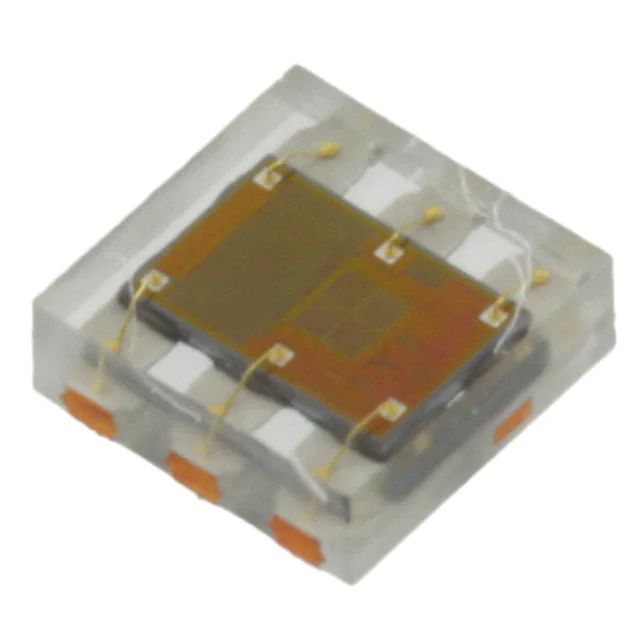
PACKAGE FN
DUAL FLAT NO-LEAD
(TOP VIEW)
D Ambient Light Sensing (ALS)
D
D
D
D
D
− Approximates Human Eye Response
− Programmable Analog Gain and
Integration Time
− 45,000,000:1 Dynamic Range
− Operation to 60,000 lux in Sunlight
− Very High Sensitivity — Ideally Suited for
Operation Behind Dark Glass
− Package UV Rejection Filter
Maskable Interrupt
− Programmable Upper and Lower
Thresholds with Persistence Filter
Wait Timer and Power Management
− Low Power 2.2 mA Sleep State with UserSelectable Sleep-After-Interrupt Mode
− 90 mA Wait State with Programmable Wait
Time from 2.7 ms to > 8 seconds
2
I C Fast Mode Compatible Interface
− Data Rates up to 400 kbit/s
− Input Voltage Levels Compatible with VDD
or 1.8-V Bus
Register Set- and Pin-Compatible with the
TSL2x71 Series
Small 2 mm � 2 mm Dual Flat No-Lead (FN)
Package
VDD 1
6 SDA
SCL 2
5 INT
GND 3
4 NC
Not Actual Size
Applications
D Display Backlight Control
D Keyboard Illumination Control
D Solid State Lighting Control for Daylight
D
Harvesting
Printer Paper Detection
End Products and Market Segments
D Mobile Handsets, Tablets, Laptops,
D
D
D
D
D
D
Monitors and TVs, Portable Media Players
Medical and Industrial Instrumentation
White Goods
Toys
Industrial/Commercial Lighting
Digital Signage
Printers
Description
The TSL2572 device family provides ambient light sensing (ALS) that approximates human eye response to
light intensity under a variety of lighting conditions and through a variety of attenuation materials. Accurate ALS
measurements are the result of TAOS’ patented dual-diode technology and the UV rejection filter incorporated
in the package. In addition, the operating range is extended to 60,000 lux in sunlight when the low-gain mode
is used.
While useful for general purpose light sensing, the TSL2572 device is particularly useful for display
management to provide optimum viewing in diverse lighting conditions while extending battery life. The
TSL2572 device family is ideally suited for use in mobile handsets, TVs, tablets, monitors, and portable media
players where the display backlight may account for 50% to 70% of the system power consumption.
The LUMENOLOGY r Company
Copyright E 2012, TAOS Inc.
r
Texas Advanced Optoelectronic Solutions Inc.
1001 Klein Road S Suite 300 S Plano, TX 75074 S (972)
r 673-0759
www.taosinc.com
1
�TSL2572
LIGHT-TO-DIGITAL CONVERTER
TAOS132 − MARCH 2012
Functional Block Diagram
Interrupt
INT
Wait Control
Upper Limit
CH0
Data
ALS Control
I2C Interface
CH0
ADC
VDD
Lower Limit
CH0
CH1
ADC
CH1
Data
SCL
SDA
GND
CH1
Detailed Description
The TSL2572 light-to-digital device provides on-chip photodiodes, integrating amplifiers, ADCs, accumulators,
clocks, buffers, comparators, a state machine, and an I2C interface. Each device combines a Channel 0
photodiode (CH0), which is responsive to both visible and infrared light, and a channel 1 photodiode (CH1),
which is responsive primarily to infrared light. Two integrating ADCs simultaneously convert the amplified
photodiode currents into a digital value providing up to 16 bits of resolution. Upon completion of the conversion
cycle, the conversion result is transferred to the data registers. This digital output can be read by a
microprocessor through which the illuminance (ambient light level) in lux is derived using an empirical formula
to approximate the human eye response.
Communication to the device is accomplished through a fast (up to 400 kHz), two-wire I2C serial bus for easy
connection to a microcontroller or embedded controller. The digital output of the device is inherently more
immune to noise when compared to an analog interface.
The device provides a separate pin for level-style interrupts. When interrupts are enabled and a pre-set value
is exceeded, the interrupt pin is asserted and remains asserted until cleared by the controlling firmware. The
interrupt feature simplifies and improves system efficiency by eliminating the need to poll a sensor for a light
intensity value. An interrupt is generated when the value of an ALS conversion exceeds either an upper or lower
threshold. In addition, a programmable interrupt persistence feature allows the user to determine how many
consecutive exceeded thresholds are necessary to trigger an interrupt.
Copyright E 2012, TAOS Inc.
The LUMENOLOGY r Company
r
r
2
www.taosinc.com
�TSL2572
LIGHT-TO-DIGITAL CONVERTER
TAOS132 − MARCH 2012
Terminal Functions
TERMINAL
TYPE
NAME
NO.
GND
3
INT
5
NC
4
SCL
2
I
SDA
6
I/O
VDD
1
DESCRIPTION
Power supply ground. All voltages are referenced to GND.
O
Interrupt — open drain (active low).
Do not connect.
I2C serial clock input terminal — clock signal for I2C serial data.
I2C serial data I/O terminal — serial data I/O for I2C .
Supply voltage.
Available Options
DEVICE
†
ADDRESS
PACKAGE − LEADS
INTERFACE DESCRIPTION
ORDERING NUMBER
TSL25721
0x39
FN−6
I2C
Vbus = VDD Interface
TSL25721FN
TSL25723
0x39
FN−6
I2C Vbus = 1.8 V Interface
TSL25723FN
TSL25725†
0x29
FN−6
I2C
Vbus = VDD Interface
TSL25725FN
TSL25727†
0x29
FN−6
I2C Vbus = 1.8 V Interface
TSL25727FN
Contact TAOS for availability.
Absolute Maximum Ratings over operating free-air temperature range (unless otherwise noted)†
Supply voltage, VDD (Note 1) . . . . . . . . . . . . . . . . . . . . . . . . . . . . . . . . . . . . . . . . . . . . . . . . . . . . . . . . . . . . . . . 3.8 V
Input terminal voltage . . . . . . . . . . . . . . . . . . . . . . . . . . . . . . . . . . . . . . . . . . . . . . . . . . . . . . . . . . . . . −0.5 V to 3.8 V
Output terminal voltage . . . . . . . . . . . . . . . . . . . . . . . . . . . . . . . . . . . . . . . . . . . . . . . . . . . . . . . . . . . −0.5 V to 3.8 V
Output terminal current . . . . . . . . . . . . . . . . . . . . . . . . . . . . . . . . . . . . . . . . . . . . . . . . . . . . . . . . . . . −1 mA to 20 mA
Storage temperature range, Tstg . . . . . . . . . . . . . . . . . . . . . . . . . . . . . . . . . . . . . . . . . . . . . . . . . . . . −40°C to 85°C
ESD tolerance, human body model . . . . . . . . . . . . . . . . . . . . . . . . . . . . . . . . . . . . . . . . . . . . . . . . . . . . . . . . . 2000 V
†
Stresses beyond those listed under “absolute maximum ratings” may cause permanent damage to the device. These are stress ratings only, and
functional operation of the device at these or any other conditions beyond those indicated under “recommended operating conditions” is not
implied. Exposure to absolute-maximum-rated conditions for extended periods may affect device reliability.
NOTE 1: All voltages are with respect to GND.
Recommended Operating Conditions
MIN
NOM
MAX
Supply voltage, VDD (TSL25721 & TSL25725) (I2C Vbus = VDD)
2.4
3
3.6
V
Supply voltage, VDD (TSL25723 & TSL25727) (I2C Vbus = 1.8 V)
2.7
3
3.6
V
Operating free-air temperature, TA
−30
70
°C
The LUMENOLOGY r Company
UNIT
Copyright E 2012, TAOS Inc.
r
r
www.taosinc.com
3
�TSL2572
LIGHT-TO-DIGITAL CONVERTER
TAOS132 − MARCH 2012
Operating Characteristics, VDD = 3 V, TA = 25�C (unless otherwise noted)
PARAMETER
TEST CONDITIONS
MIN
Active
IDD
Supply current
VOL
INT SDA output low voltage
INT,
I LEAK
Leakage current, SDA, SCL, INT pins
VIH
SCL SDA input high voltage
SCL,
VIL
SCL SDA input low voltage
SCL,
TYP
MAX
200
250
Wait state
90
Sleep state — no I2C activity
2.2
μA
4
3 mA sink current
0
0.4
6 mA sink current
0
0.6
−5
5
TSL25721, TSL25725
0.7 VDD
TSL25723, TSL25727
1.25
UNIT
V
μA
V
TSL25721, TSL25725
0.3 VDD
TSL25723, TSL25727
0.54
V
ALS Characteristics, VDD = 3 V, TA = 25�C, AGAIN = 16�, AEN = 1 (unless otherwise noted)
(Notes 1 ,2, 3)
PARAMETER
TEST CONDITIONS
Dark ADC count value
Ee = 0, AGAIN = 120×,
ATIME = 0xDB (100 ms)
ADC integration time step size
ATIME = 0xFF
CHANNEL
MIN
TYP
MAX
CH0
0
1
5
CH1
0
1
5
2.58
2.73
2.9
ms
256
steps
ADC number of integration steps
(Note 4)
counts
ADC counts per step (Note 4)
ATIME = 0xFF
0
1024
counts
ADC count value (Note 4)
ATIME = 0xC0
0
65535
counts
ADC count value
ADC count value ratio: CH1/CH0
Re
1
UNIT
Irradiance responsivity
White light, Ee = 263.9 μW/cm2,
ATIME = 0xF6 (27 ms) (Note 2)
CH0
λp = 850 nm, Ee = 263.4 μW/cm2,
ATIME = 0xF6 (27 ms) (Note 3)
CH0
5000
6000
680
4000
5000
White light, ATIME = 0xF6 (27 ms) (Note 2)
0.086
0.136
0.186
λp = 850 nm, ATIME = 0xF6 (27 ms) (Note 3)
0.456
0.570
0.684
CH1
6000
CH0
18.9
CH1
2.58
λp = 850 nm, ATIME = 0xF6 (27 ms)
(Note 3)
CH0
19.0
CH1
counts/
(μW/
cm2)
10.8
0.128
0.16
0.192
AGAIN = 8× and AGL = 0
7.2
8.0
8.8
AGAIN = 16× and AGL = 0
14 4
14.4
16 0
16.0
17
17.6
6
108
120
132
AGAIN = 120× and AGL = 0
counts
2850
White light, ATIME = 0xF6 (27 ms)
(Note 2)
AGAIN = 1× and AGL = 1
Gain scaling, relative to 1× gain
setting
4000
CH1
×
NOTES: 1. Optical measurements are made using small-angle incident radiation from light-emitting diode optical sources. Visible white LEDs
and infrared 850 nm LEDs are used for final product testing for compatibility with high-volume production.
2. The white LED irradiance is supplied by a white light-emitting diode with a nominal color temperature of 4000 K.
3. The 850 nm irradiance Ee is supplied by a GaAs light-emitting diode with the following typical characteristics: peak wavelength
λp = 850 nm and spectral halfwidth Δλ½ = 42 nm.
4. Parameter ensured by design and is not tested.
Copyright E 2012, TAOS Inc.
The LUMENOLOGY r Company
r
r
4
www.taosinc.com
�TSL2572
LIGHT-TO-DIGITAL CONVERTER
TAOS132 − MARCH 2012
Wait Characteristics, VDD = 3 V, TA = 25�C, WEN = 1 (unless otherwise noted)
PARAMETER
TEST CONDITIONS
Wait step size
CHANNEL
WTIME = 0xFF
Wait number of integration steps (Note 1)
MIN
TYP
2.58
2.73
1
MAX
UNIT
2.9
ms
256
steps
NOTE 1: Parameter ensured by design and is not tested.
AC Electrical Characteristics, VDD = 3 V, TA = 25�C (unless otherwise noted)
PARAMETER†
†
(I2C
TEST CONDITIONS
MIN
only)
TYP
0
MAX
UNIT
400
kHz
f(SCL)
Clock frequency
t(BUF)
Bus free time between start and stop condition
1.3
μs
t(HDSTA)
Hold time after (repeated) start condition. After
this period, the first clock is generated.
0.6
μs
t(SUSTA)
Repeated start condition setup time
0.6
μs
t(SUSTO)
Stop condition setup time
0.6
μs
t(HDDAT)
Data hold time
0
μs
t(SUDAT)
Data setup time
100
ns
t(LOW)
SCL clock low period
1.3
μs
t(HIGH)
SCL clock high period
0.6
tF
Clock/data fall time
300
ns
tR
Clock/data rise time
300
ns
Ci
Input pin capacitance
10
pF
μs
Specified by design and characterization; not production tested.
PARAMETER MEASUREMENT INFORMATION
t(LOW)
t(R)
t(F)
VIH
SCL
VIL
t(HDSTA)
t(BUF)
t(HIGH)
t(HDDAT)
t(SUSTA)
t(SUSTO)
t(SUDAT)
VIH
SDA
VIL
P
Stop
Condition
S
S
P
Start
Condition
Figure 1. Timing Diagrams
The LUMENOLOGY r Company
Copyright E 2012, TAOS Inc.
r
r
www.taosinc.com
5
�TSL2572
LIGHT-TO-DIGITAL CONVERTER
TAOS132 − MARCH 2012
TYPICAL CHARACTERISTICS
NORMALIZED RESPONSIVITY
vs.
ANGULAR DISPLACEMENT
SPECTRAL RESPONSIVITY
1.0
1
Both Axes
Ch 0
Normalized Responsivity
Normalized Responsivity
0.6
0.4
Ch 1
0.6
0.4
0.2
0
300
Optical Axis
0.8
0.8
0.2
400
500
600
700
800
0
−90
900 1000 1100
λ − Wavelength − nm
-Q
115%
Response — Normalized to 25° C
IDD — Active Current Normalized @ 3 V, 25�C
RESPONSE to WHITE LED
vs.
TEMPERATURE
NORMALIZED IDD
vs.
VDD and TEMPERATURE
108%
106%
104%
0�C
102%
100%
50�C
25�C
75�C
98%
96%
110%
105%
Ch 0
100%
95%
Ch 1
94%
92%
2.7
90%
2.8
2.9
3
3.1
3.2
3.3
0
10
20
VDD — V
Figure 4
Copyright E 2012, TAOS Inc.
30
40
50
Temperature − °C
60
70
Figure 5
The LUMENOLOGY r Company
r
r
6
90
Figure 3
Figure 2
110%
+Q
−60
−30
0
30
60
Q − Angular Displacement − °
www.taosinc.com
�TSL2572
LIGHT-TO-DIGITAL CONVERTER
TAOS132 − MARCH 2012
PRINCIPLES OF OPERATION
System State Machine
An internal state machine provides system control of the ALS and wait timer features of the device. At power
up, an internal power-on-reset initializes the device and puts it in a low-power Sleep state.
When a start condition is detected on the I2C bus, the device transitions to the Idle state where it checks the
Enable register (0x00) PON bit. If PON is disabled, the device will return to the Sleep state to save power.
Otherwise, the device will remain in the Idle state until the ALS function is enabled. Once enabled, the device
will execute the Wait and ALS states in sequence as indicated in Figure 6. Upon completion and return to Idle,
the device will automatically begin a new Wait-ALS cycle as long as PON and AEN remain enabled.
If the ALS function generates an interrupt and the Sleep-After-Interrupt (SAI) feature is enabled, the device will
transition to the Sleep state and remain in a low-power mode until an I2C command is received. See the
Interrupts section for additional information.
Sleep
I2C
Start
!PON
Idle
WEN &
AEN
!WEN
& AEN
Wait
INT & SAI
ALS
Figure 6. Simplified State Diagram
Photodiodes
Conventional ALS detectors respond strongly to infrared light, which the human eye does not see. This can lead
to significant error when the infrared content of the ambient light is high (such as with incandescent lighting).
This problem is overcome through the use of two photodiodes. The Channel 0 photodiode, referred to as the
CH0 channel, is sensitive to both visible and infrared light, while the Channel 1 photodiode, referred to as CH1,
is sensitive primarily to infrared light. Two integrating ADCs convert the photodiode currents to digital outputs.
The ADC digital outputs from the two channels are used in a formula to obtain a value that approximates the
human eye response in units of lux.
The LUMENOLOGY r Company
Copyright E 2012, TAOS Inc.
r
r
www.taosinc.com
7
�TSL2572
LIGHT-TO-DIGITAL CONVERTER
TAOS132 − MARCH 2012
ALS Operation
The ALS engine contains ALS gain control (AGAIN) and two integrating analog-to-digital converters (ADC), one
for the CH0 and one for the CH1 photodiodes. The ALS integration time (ATIME) impacts both the resolution
and the sensitivity of the ALS reading. Integration of both channels occurs simultaneously and upon completion
of the conversion cycle, the results are transferred to the data registers (C0DATA and C1DATA). This data is
also referred to as channel count. The transfers are double-buffered to ensure data integrity.
ATIME(r 1)
2.73 ms to 699 ms
CH0
ALS
CH0
Data
ALS Control
C0DATAH(r0x15), C0DATA(r0x14)
AGL(r0x0D, b2)
CH0
CH1
ADC
CH1
Data
C1DATAH(r0x17), C1DATA(r0x16)
CH1
AGAIN(r0x0F, b1:0)
1�, 8�, 16�, 120� Gain
Figure 7. ALS Operation
The registers for programming the integration and wait times are 2’s compliment values. The actual time can
be calculated as follows:
ATIME = 256 − Integration Time / 2.73 ms
Inversely, the time can be calculated from the register value as follows:
Integration Time = 2.73 ms × (256 − ATIME)
In order to reject the 50/60-Hz ripple present in fluorescent lighting, the integration time needs to
be programmed in multiples of 10 / 8.3 ms or the half cycle time. Both frequencies can be rejected with a
programmed value of 50 ms (ATIME = 0xED) or multiples of 50 ms (i.e. 100, 150, 200, 400, 600).
AGAIN can be programmed to 1×, 8×, 16×, or 120× with the 2-bit AGAIN field in the Control register (0x0F).
The gain, in terms of amount of gain, will be represented by the value AGAINx, i.e. AGAINx = 1, 8, 16, or 120.
With the AGL bit set, the 1× and 8× gains are lowered to 1/6× and 8/6×, respectively, to allow for operation up
to 60k lux. Do not enable AGL when AGAIN is 16× or 120×.
Lux Equation
The lux calculation is a function of CH0 channel count (C0DATA), CH1 channel count (C1DATA), ALS gain
(AGAINx), and ALS integration time in milliseconds (ATIME_ms). If an aperture, glass/plastic, or a light pipe
attenuates the light equally across the spectrum (300 nm to 1100 nm), then a scaling factor referred to as glass
attenuation (GA) can be used to compensate for attenuation. For a device in open air with no aperture or
glass/plastic above the device, GA = 1. If it is not spectrally flat, then a custom lux equation with new coefficients
should be generated. (See TAOS application note).
Counts per Lux (CPL) needs to be calculated only when ATIME or AGAIN is changed, otherwise it remains a
constant. The first segment of the equation (Lux1) covers fluorescent and incandescent light. The second
segment (Lux2) covers dimmed incandescent light. The final lux is the maximum of Lux1, Lux2, or 0.
CPL = (ATIME_ms × AGAINx) / (GA × 60)
Lux1 = (1 × C0DATA − 1.87 × C1DATA) / CPL
Lux2 = (0.63 × C0DATA − 1 × C1DATA) / CPL
Lux = MAX(Lux1, Lux2, 0)
Copyright E 2012, TAOS Inc.
The LUMENOLOGY r Company
r
r
8
www.taosinc.com
�TSL2572
LIGHT-TO-DIGITAL CONVERTER
TAOS132 − MARCH 2012
Interrupts
The interrupt feature simplifies and improves system efficiency by eliminating the need to poll the sensor for
light intensity values outside of a user-defined range. While the interrupt function is always enabled and it’s
status is available in the status register (0x13), the output of the interrupt state can be enabled using the ALS
interrupt enable (AIEN) fields in the enable register (0x00).
Two 16-bit interrupt threshold registers allow the user to set limits below and above a desired light level. An
interrupt can be generated when the ALS CH0 data (C0DATA) falls outside of the desired light level range, as
determined by the values in the ALS interrupt low threshold registers (AILTx) and ALS interrupt high threshold
registers (AIHTx).
It is important to note that the thresholds are evaluated in sequence, first the low threshold, then the high
threshold. As a result, if the low threshold is set above the high threshold, the high threshold is ignored and only
the low threshold is evaluated.
To further control when an interrupt occurs, the device provides a persistence filter. The persistence filter allows
the user to specify the number of consecutive out-of-range ALS occurrences before an interrupt is generated.
The persistence filter register (0x0C) allows the user to set the ALS persistence filter (APERS) value. See the
persistence filter register for details on the persistence filter values. Once the persistence filter generates an
interrupt, it will continue until a special function interrupt clear command is received (see command register).
AIHTH(r07), AIHTL(r06)
Upper Limit
CH0
ADC
APERS(r0x0C, b3:0)
ALS Persistence
CH0
Data
Lower Limit
CH0
AILTH(r05), AILTL(r04)
Figure 8. Programmable Interrupt
The LUMENOLOGY r Company
Copyright E 2012, TAOS Inc.
r
r
www.taosinc.com
9
�TSL2572
LIGHT-TO-DIGITAL CONVERTER
TAOS132 − MARCH 2012
System State Machine Timing
The system state machine shown in Figure 6 provides an overview of the states and state transitions that
provide system control of the device. This section highlights the programmable features, which affect the state
machine cycle time, and provides details to determine system level timing.
When the power management feature is enabled (WEN), the state machine will transition in turn to the Wait
state. The wait time is determined by WLONG, which extends normal operation by 12× when asserted, and
WTIME. The formula to determine the wait time is given in the box associated with the Wait state in Figure 9.
When the ALS feature is enabled (AEN), the state machine will transition through the ALS Init and ALS ADC
states. The ALS Init state takes 2.73 ms, while the ALS ADC time is dependent on the integration time (ATIME).
The formula to determine ALS ADC time is given in the associated box in Figure 9. If an interrupt is generated
as a result of the ALS cycle, it will be asserted at the end of the ALS ADC state and transition to the Sleep state
if SAI is enabled.
Sleep
I2C Start
!PON
WEN
& AEN
Idle
INT & SAI
!WEN
& AEN
ALS
ADC
Wait
ATIME: 1 ~ 256 steps
Time: 2.73 ms/step
Range: 2.73 ms ~ 699 ms
ALS
Init
Time:
Range:
WTIME: 1 ~ 256 steps
WLONG = 0
WLONG = 1
2.73 ms/step
32.8 ms/step
2.73 ms ~ 699 ms
32.8 ms ~ 8.39s
Time: 2.73 ms
Note: PON, WEN, AEN, and SAI are fields in the Enable register (0x00).
Figure 9. Detailed State Diagram
Copyright E 2012, TAOS Inc.
The LUMENOLOGY r Company
r
r
10
www.taosinc.com
�TSL2572
LIGHT-TO-DIGITAL CONVERTER
TAOS132 − MARCH 2012
I2C Protocol
Interface and control are accomplished through an I2C serial compatible interface (standard or fast mode) to
a set of registers that provide access to device control functions and output data. The devices support the 7-bit
I2C addressing protocol.
The I2C standard provides for three types of bus transaction: read, write, and a combined protocol (Figure 10).
During a write operation, the first byte written is a command byte followed by data. In a combined protocol, the
first byte written is the command byte followed by reading a series of bytes. If a read command is issued, the
register address from the previous command will be used for data access. Likewise, if the MSB of the command
is not set, the device will write a series of bytes at the address stored in the last valid command with a register
address. The command byte contains either control information or a 5-bit register address. The control
commands can also be used to clear interrupts.
The I2C bus protocol was developed by Philips (now NXP). For a complete description of the I2C protocol, please
review the NXP I2C design specification at http://www.i2c−bus.org/references/.
A
N
P
R
S
Sr
W
...
Acknowledge (0)
Not Acknowledged (1)
Stop Condition
Read (1)
Start Condition
Repeated Start Condition
Write (0)
Continuation of protocol
Master-to-Slave
Slave-to-Master
1
S
7
1
Slave Address
W
1
8
A
1
Command Code
8
A
1
Data Byte
A
1
8
1
A
Data
A
1
...
P
I2C Write Protocol
1
7
1
1
S
Slave Address
R
A
8
Data
1
...
P
I2C Read Protocol
1
7
1
1
8
1
1
7
1
1
S
Slave Address
W
A
Command Code
A
Sr
Slave Address
R
A
8
1
Data
A
8
Data
1
A
1
...
P
I2C Read Protocol — Combined Format
Figure 10. I2C Protocols
The LUMENOLOGY r Company
Copyright E 2012, TAOS Inc.
r
r
www.taosinc.com
11
�TSL2572
LIGHT-TO-DIGITAL CONVERTER
TAOS132 − MARCH 2012
Register Set
The device is controlled and monitored by data registers and a command register accessed through the serial
interface. These registers provide for a variety of control functions and can be read to determine results of the
ADC conversions. The register set is summarized in Table 1.
Table 1. Register Address
ADDRESS
RESISTER NAME
R/W
−−
COMMAND
W
0x00
ENABLE
0x01
0x03
0x04
0x05
0x06
REGISTER FUNCTION
RESET VALUE
Specifies register address
0x00
R/W
Enables states and interrupts
0x00
ATIME
R/W
ALS time
0xFF
WTIME
R/W
Wait time
0xFF
AILTL
R/W
ALS interrupt low threshold low byte
0x00
AILTH
R/W
ALS interrupt low threshold high byte
0x00
AIHTL
R/W
ALS interrupt high threshold low byte
0x00
0x07
AIHTH
R/W
ALS interrupt high threshold high byte
0x00
0x0C
PERS
R/W
Interrupt persistence filters
0x00
0x0D
CONFIG
R/W
Configuration
0x00
0x0F
CONTROL
R/W
Control register
0x00
0x12
ID
R
Device ID
0x13
STATUS
R
Device status
0x00
0x14
C0DATA
R
CH0 ADC low data register
0x00
0x15
C0DATAH
R
CH0 ADC high data register
0x00
0x16
C1DATA
R
CH1 ADC low data register
0x00
0x17
C1DATAH
R
CH1 ADC high data register
0x00
ID
The mechanics of accessing a specific register depends on the specific protocol used. See the section on I2C
protocols on the previous pages. In general, the COMMAND register is written first to specify the specific
control/status register for following read/write operations.
Copyright E 2012, TAOS Inc.
The LUMENOLOGY r Company
r
r
12
www.taosinc.com
�TSL2572
LIGHT-TO-DIGITAL CONVERTER
TAOS132 − MARCH 2012
Command Register
The command registers specifies the address of the target register for future write and read operations.
Table 2. Command Register
7
6
COMMAND
COMMAND
FIELD
BITS
COMMAND
7
TYPE
6:5
5
4
3
TYPE
2
1
0
Reset
0x00
ADD
DESCRIPTION
Select Command Register. Must write as 1 when addressing COMMAND register.
Selects type of transaction to follow in subsequent data transfers:
FIELD VALUE
DESCRIPTION
00
Repeated byte protocol transaction
01
Auto-increment protocol transaction
10
Reserved — Do not use
11
Special function — See description below
Transaction type 00 will repeatedly read the same register with each data access.
Transaction type 01 will provide an auto-increment function to read successive register bytes.
ADD
4:0
Address field/special function field. Depending on the transaction type, see above, this field either
specifies a special function command or selects the specific control-status-register for following write and
read transactions. The field values listed below apply only to special function commands:
FIELD VALUE
DESCRIPTION
00000
Normal — no action
00110
ALS interrupt clear
other
Reserved — Do not write
The ALS interrupt clear special function clears any pending ALS interrupt and is self clearing.
The LUMENOLOGY r Company
Copyright E 2012, TAOS Inc.
r
r
www.taosinc.com
13
�TSL2572
LIGHT-TO-DIGITAL CONVERTER
TAOS132 − MARCH 2012
Enable Register (0x00)
The ENABLE register is used to power the device on/off, enable functions, and interrupts.
Table 3. Enable Register
ENABLE
7
6
5
4
3
2
1
0
Reserved
SAI
Reserved
Resv
AIEN
WEN
Reserved
AEN
PON
Reset
0x00
FIELD
BITS
Reserved
7
Reserved. Write as 0.
SAI
6
Sleep after interrupt. When asserted, the device will power down at the end of an ALS cycle if an interrupt has
been generated.
Reserved
5
Reserved. Write as 0.
AIEN
4
ALS interrupt mask. When asserted, permits ALS interrupts to be generated.
WEN
3
Wait Enable. This bit activates the wait feature. Writing a 1 activates the wait timer. Writing a 0 disables the
wait timer.
Reserved
2
Reserved. Write as 0.
AEN
1
ALS Enable. This bit actives the two channel ADC. Writing a 1 activates the ALS. Writing a 0 disables the ALS.
PON
0
Power ON. This bit activates the internal oscillator to permit the timers and ADC channels to operate. Writing a
1 activates the oscillator. Writing a 0 disables the oscillator.
DESCRIPTION
ALS Time Register (0x01)
The ALS time register controls the internal integration time of the ALS channel ADCs in 2.73 ms increments.
Upon power up, the ALS time register is set to 0xFF.
Table 4. ALS Time Register
FIELD
BITS
ATIME
7:0
DESCRIPTION
VALUE
INTEG_CYCLES
TIME
0xFF
1
2.73 ms
MAX COUNT
1024
0xF6
10
27.3 ms
10240
0xDB
37
101 ms
37888
0xC0
64
175 ms
65535
0x00
256
699 ms
65535
Wait Time Register (0x03)
Wait time is set 2.73 ms increments unless the WLONG bit is asserted in which case the wait times are 12×
longer. WTIME is programmed as a 2’s complement number. Upon power up, the wait time register is set to
0xFF.
Table 5. Wait Time Register
FIELD
BITS
WTIME
7:0
DESCRIPTION
REGISTER VALUE
WAIT TIME
TIME (WLONG = 0)
TIME (WLONG = 1)
0xFF
1
2.73 ms
0.033 sec
0xB6
74
202 ms
2.4 sec
0x00
256
699 ms
8.4 sec
NOTE: The Wait Time Register should be configured before AEN is asserted.
Copyright E 2012, TAOS Inc.
The LUMENOLOGY r Company
r
r
14
www.taosinc.com
�TSL2572
LIGHT-TO-DIGITAL CONVERTER
TAOS132 − MARCH 2012
ALS Interrupt Threshold Registers (0x04 − 0x07)
The ALS interrupt threshold registers provides the values to be used as the high and low trigger points for the
comparison function for interrupt generation. If C0DATA crosses below the low threshold specified, or above
the higher threshold, an interrupt is asserted on the interrupt pin.
Table 6. ALS Interrupt Threshold Registers
REGISTER
ADDRESS
BITS
AILTL
0x04
7:0
ALS low threshold lower byte
DESCRIPTION
AILTH
0x05
7:0
ALS low threshold upper byte
AIHTL
0x06
7:0
ALS high threshold lower byte
AIHTH
0x07
7:0
ALS high threshold upper byte
Persistence Filter Register (0x0C)
The persistence filter register controls the interrupt capabilities of the device. Configurable filtering is provided
to allow interrupts to be generated after every ADC cycle or if the ADC cycle has produced a result that is outside
of the values specified by threshold register for some specified amount of time. ALS interrupts are generated
using C0DATA.
Table 7. Persistence Filter Register
7
6
PERS
5
4
3
Reserved
2
1
0
Reset
0x00
APERS
FIELD
BITS
Reserved
7:4
Reserved. Write as 0.
APERS
3:0
ALS Interrupt persistence filter. Controls rate of ALS interrupt to the host processor.
The LUMENOLOGY r Company
DESCRIPTION
FIELD VALUE
MEANING
INTERRUPT PERSISTENCE FUNCTION
0000
Every
0001
1
1 value outside of threshold range
0010
2
2 consecutive values out of range
Every ALS cycle generates an interrupt
0011
3
3 consecutive values out of range
0100
5
5 consecutive values out of range
0101
10
10 consecutive values out of range
0110
15
15 consecutive values out of range
0111
20
20 consecutive values out of range
1000
25
25 consecutive values out of range
1001
30
30 consecutive values out of range
1010
35
35 consecutive values out of range
1011
40
40 consecutive values out of range
1100
45
45 consecutive values out of range
1101
50
50 consecutive values out of range
1110
55
55 consecutive values out of range
1111
60
60 consecutive values out of range
Copyright E 2012, TAOS Inc.
r
r
www.taosinc.com
15
�TSL2572
LIGHT-TO-DIGITAL CONVERTER
TAOS132 − MARCH 2012
Configuration Register (0x0D)
The configuration register sets the wait long time and ALS gain level.
Table 8. Configuration Register
7
6
5
CONFIG
4
3
Reserved
2
1
0
AGL
WLONG
Reserved
Reset
0x00
FIELD
BITS
Reserved
7:3
DESCRIPTION
AGL
2
ALS gain level. When asserted, the 1× and 8× ALS gain (AGAIN) modes are scaled by 0.16. Otherwise,
AGAIN is scaled by 1. Do not use with AGAIN greater than 8×.
WLONG
1
Wait Long. When asserted, the wait cycles are increased by a factor 12× from that programmed in the
WTIME register.
Reserved
0
Reserved. Write as 0.
Reserved. Write as 0.
Control Register (0x0F)
The Control register provides ALS gain control to the analog block.
Table 9. Control Register
7
6
5
CONTROL
4
3
2
1
0
FIELD
BITS
Reserved
7:2
Reserved. Write as 0.
AGAIN
1:0
ALS Gain.
Reset
0x00
AGAIN
Reserved
DESCRIPTION
FIELD VALUE
ALS GAIN VALUE
00
1× gain
01
8× gain
10
16× gain
11
120× gain
ID Register (0x12)
The ID Register provides the value for the part number. The ID register is a read-only register.
Table 10. ID Register
7
6
5
ID
4
3
2
1
Reset
ID
ID
FIELD
BITS
ID
7:0
0
DESCRIPTION
0x34= TSL25721 & TSL25725
Copyright E 2012, TAOS Inc.
Part number identification
0x3D = TSL25723 & TSL25727
The LUMENOLOGY r Company
r
r
16
www.taosinc.com
�TSL2572
LIGHT-TO-DIGITAL CONVERTER
TAOS132 − MARCH 2012
Status Register (0x13)
The Status Register provides the internal status of the device. This register is read only.
Table 11. Status Register
7
STATUS
6
5
Reserved
FIELD
BIT
Reserved
7:5
AINT
4
Reserved
3:1
AVALID
0
4
3
AINT
2
1
Reserved
0
AVALID
Reset
0x00
DESCRIPTION
Reserved. Bits read as 0.
ALS Interrupt. Indicates that the device is asserting an ALS interrupt.
Reserved. Bits read as 0.
ALS Valid. Indicates that the ALS channels have completed an integration cycle after AEN has been
asserted.
ADC Channel Data Registers (0x14 − 0x17)
ALS data is stored as two 16-bit values. To ensure the data is read correctly, a two-byte read I2C transaction
should be used with auto increment protocol bits set in the command register. With this operation, when the
lower byte register is read, the upper eight bits are stored in a shadow register, which is read by a subsequent
read to the upper byte. The upper register will read the correct value even if additional ADC integration cycles
end between the reading of the lower and upper registers.
Table 12. ADC Channel Data Registers
REGISTER
ADDRESS
BITS
DESCRIPTION
C0DATA
0x14
7:0
ALS CH0 data low byte
C0DATAH
0x15
7:0
ALS CH0 data high byte
C1DATA
0x16
7:0
ALS CH1 data low byte
C1DATAH
0x17
7:0
ALS CH1 data high byte
The LUMENOLOGY r Company
Copyright E 2012, TAOS Inc.
r
r
www.taosinc.com
17
�TSL2572
LIGHT-TO-DIGITAL CONVERTER
TAOS132 − MARCH 2012
APPLICATION INFORMATION: HARDWARE
Typical Hardware Application
A typical hardware application circuit is shown in Figure 11. A 1-μF low-ESR decoupling capacitor should be
placed as close as possible to the VDD pin.
VDD
VBUS
VDD
RP
1 mF
TSL2572
RP
RPI
INT
SCL
GND
SDA
Figure 11. Typical Application Hardware Circuit
VBUS in Figure 11 refers to the I2C bus voltage, which is either VDD or 1.8 V. Be sure to apply the specified I2C
bus voltage shown in the Available Options table for the specific device being used.
The I2C signals and the Interrupt are open-drain outputs and require pull-up resistors. The pull-up resistor (RP)
value is a function of the I2C bus speed, the I2C bus voltage, and the capacitive load. The TAOS EVM running
at 400 kbps, uses 1.5-kΩ resistors. A 10-kΩ pull-up resistor (RPI) can be used for the interrupt line.
PCB Pad Layout
Suggested land pattern based on the IPC−7351B Generic Requirements for Surface Mount Design and Land
Pattern Standard (2010) for the small outline no-lead (SON) package is shown in Figure 12.
2.70
1.20
1.20
0.35 � 6
0.65
0.65
TOP VIEW
NOTES: A. All linear dimensions are in millimeters.
B. This drawing is subject to change without notice.
Figure 12. Suggested FN Package PCB Layout
Copyright E 2012, TAOS Inc.
The LUMENOLOGY r Company
r
r
18
www.taosinc.com
�TSL2572
LIGHT-TO-DIGITAL CONVERTER
TAOS132 − MARCH 2012
PACKAGE INFORMATION
PACKAGE FN
Dual Flat No-Lead
TOP VIEW
398 � 10
PIN OUT
TOP VIEW
PIN 1
355
� 10
2000 � 100
2000
� 100
VDD 1
6 SDA
SCL 2
5 INT
GND 3
4 NC
Photodiode Array Area
END VIEW
SIDE VIEW
295
Nominal
650 � 50
203 � 8
650
BSC
BOTTOM VIEW
CL
of Photodiode Array Area
(Note B)
300
� 50
CL of Solder Contacts
1 Nominal
144 Nominal
CL of Solder Contacts
CL of Photodiode Array Area (Note B)
PIN 1
Pb
750 � 150
NOTES: A.
B.
C.
D.
E.
F.
Lead Free
All linear dimensions are in micrometers.
The die is centered within the package within a tolerance of ± 75 μm.
Package top surface is molded with an electrically nonconductive clear plastic compound having an index of refraction of 1.55.
Contact finish is copper alloy A194 with pre-plated NiPdAu lead finish.
This package contains no lead (Pb).
This drawing is subject to change without notice.
Figure 13. Package FN — Dual Flat No-Lead Packaging Configuration
The LUMENOLOGY r Company
Copyright E 2012, TAOS Inc.
r
r
www.taosinc.com
19
�TSL2572
LIGHT-TO-DIGITAL CONVERTER
TAOS132 − MARCH 2012
CARRIER TAPE AND REEL INFORMATION
TOP VIEW
2.00 � 0.05
1.75
4.00
� 1.50
4.00
B
+ 0.30
8.00
− 0.10
3.50 � 0.05
� 1.00
� 0.25
A
B
A
DETAIL A
DETAIL B
5� Max
5� Max
0.254
� 0.02
2.18 � 0.05
NOTES: A.
B.
C.
D.
E.
F.
G.
2.18 � 0.05
0.83 � 0.05
Ao
Bo
Ko
All linear dimensions are in millimeters. Dimension tolerance is ± 0.10 mm unless otherwise noted.
The dimensions on this drawing are for illustrative purposes only. Dimensions of an actual carrier may vary slightly.
Symbols on drawing Ao, Bo, and Ko are defined in ANSI EIA Standard 481−B 2001.
Each reel is 178 millimeters in diameter and contains 3500 parts.
TAOS packaging tape and reel conform to the requirements of EIA Standard 481−B.
In accordance with EIA standard, device pin 1 is located next to the sprocket holes in the tape.
This drawing is subject to change without notice.
Figure 14. Package FN Carrier Tape
Copyright E 2012, TAOS Inc.
The LUMENOLOGY r Company
r
r
20
www.taosinc.com
�TSL2572
LIGHT-TO-DIGITAL CONVERTER
TAOS132 − MARCH 2012
SOLDERING INFORMATION
The FN package has been tested and has demonstrated an ability to be reflow soldered to a PCB substrate.
The solder reflow profile describes the expected maximum heat exposure of components during the solder
reflow process of product on a PCB. Temperature is measured on top of component. The components should
be limited to a maximum of three passes through this solder reflow profile.
Table 13. Solder Reflow Profile
PARAMETER
REFERENCE
DEVICE
Average temperature gradient in preheating
Soak time
2.5°C/sec
tsoak
2 to 3 minutes
Time above 217°C (T1)
t1
Max 60 sec
Time above 230°C (T2)
t2
Max 50 sec
t3
Max 10 sec
Time above Tpeak −10°C (T3)
Peak temperature in reflow
Tpeak
260°C
Temperature gradient in cooling
Tpeak
Max −5°C/sec
Not to scale — for reference only
T3
T2
Temperature (�C)
T1
Time (sec)
t3
t2
tsoak
t1
Figure 15. Solder Reflow Profile Graph
The LUMENOLOGY r Company
Copyright E 2012, TAOS Inc.
r
r
www.taosinc.com
21
�TSL2572
LIGHT-TO-DIGITAL CONVERTER
TAOS132 − MARCH 2012
STORAGE INFORMATION
Moisture Sensitivity
Optical characteristics of the device can be adversely affected during the soldering process by the release and
vaporization of moisture that has been previously absorbed into the package. To ensure the package contains
the smallest amount of absorbed moisture possible, each device is baked prior to being dry packed for shipping.
Devices are dry packed in a sealed aluminized envelope called a moisture-barrier bag with silica gel to protect
them from ambient moisture during shipping, handling, and storage before use.
Shelf Life
The calculated shelf life of the device in an unopened moisture barrier bag is 12 months from the date code on
the bag when stored under the following conditions:
Shelf Life: 12 months
Ambient Temperature: < 40°C
Relative Humidity: < 90%
Rebaking of the devices will be required if the devices exceed the 12 month shelf life or the Humidity Indicator
Card shows that the devices were exposed to conditions beyond the allowable moisture region.
Floor Life
The FN package has been assigned a moisture sensitivity level of MSL 3. As a result, the floor life of devices
removed from the moisture barrier bag is 168 hours from the time the bag was opened, provided that the devices
are stored under the following conditions:
Floor Life: 168 hours
Ambient Temperature: < 30°C
Relative Humidity: < 60%
If the floor life or the temperature/humidity conditions have been exceeded, the devices must be rebaked prior
to solder reflow or dry packing.
Rebaking Instructions
When the shelf life or floor life limits have been exceeded, rebake at 50°C for 12 hours.
Copyright E 2012, TAOS Inc.
The LUMENOLOGY r Company
r
r
22
www.taosinc.com
�TSL2572
LIGHT-TO-DIGITAL CONVERTER
TAOS132 − MARCH 2012
PRODUCTION DATA — information in this document is current at publication date. Products conform to
specifications in accordance with the terms of Texas Advanced Optoelectronic Solutions, Inc. standard
warranty. Production processing does not necessarily include testing of all parameters.
LEAD-FREE (Pb-FREE) and GREEN STATEMENT
Pb-Free (RoHS) TAOS’ terms Lead-Free or Pb-Free mean semiconductor products that are compatible with the current
RoHS requirements for all 6 substances, including the requirement that lead not exceed 0.1% by weight in homogeneous
materials. Where designed to be soldered at high temperatures, TAOS Pb-Free products are suitable for use in specified
lead-free processes.
Green (RoHS & no Sb/Br) TAOS defines Green to mean Pb-Free (RoHS compatible), and free of Bromine (Br) and
Antimony (Sb) based flame retardants (Br or Sb do not exceed 0.1% by weight in homogeneous material).
Important Information and Disclaimer The information provided in this statement represents TAOS’ knowledge and
belief as of the date that it is provided. TAOS bases its knowledge and belief on information provided by third parties,
and makes no representation or warranty as to the accuracy of such information. Efforts are underway to better integrate
information from third parties. TAOS has taken and continues to take reasonable steps to provide representative
and accurate information but may not have conducted destructive testing or chemical analysis on incoming materials and
chemicals. TAOS and TAOS suppliers consider certain information to be proprietary, and thus CAS numbers and other
limited information may not be available for release.
NOTICE
Texas Advanced Optoelectronic Solutions, Inc. (TAOS) reserves the right to make changes to the products contained in this
document to improve performance or for any other purpose, or to discontinue them without notice. Customers are advised
to contact TAOS to obtain the latest product information before placing orders or designing TAOS products into systems.
TAOS assumes no responsibility for the use of any products or circuits described in this document or customer product
design, conveys no license, either expressed or implied, under any patent or other right, and makes no representation that
the circuits are free of patent infringement. TAOS further makes no claim as to the suitability of its products for any particular
purpose, nor does TAOS assume any liability arising out of the use of any product or circuit, and specifically disclaims any
and all liability, including without limitation consequential or incidental damages.
TEXAS ADVANCED OPTOELECTRONIC SOLUTIONS, INC. PRODUCTS ARE NOT DESIGNED OR INTENDED FOR
USE IN CRITICAL APPLICATIONS IN WHICH THE FAILURE OR MALFUNCTION OF THE TAOS PRODUCT MAY
RESULT IN PERSONAL INJURY OR DEATH. USE OF TAOS PRODUCTS IN LIFE SUPPORT SYSTEMS IS EXPRESSLY
UNAUTHORIZED AND ANY SUCH USE BY A CUSTOMER IS COMPLETELY AT THE CUSTOMER’S RISK.
LUMENOLOGY, TAOS, the TAOS logo, and Texas Advanced Optoelectronic Solutions are registered trademarks of Texas Advanced
Optoelectronic Solutions Incorporated.
The LUMENOLOGY r Company
Copyright E 2012, TAOS Inc.
r
r
www.taosinc.com
23
�TSL2572
LIGHT-TO-DIGITAL CONVERTER
TAOS132 − MARCH 2012
Copyright E 2012, TAOS Inc.
The LUMENOLOGY r Company
r
r
24
www.taosinc.com
�