AS7211
Smart Lighting Manager with
Integrated Daylight Sensor, Control
Interfaces and Network Access
General Description
The AS7211 Smart Lighting Manager device is an intelligent, photopic-sensor based
light manager that enables automatic daylight level adaptation and energy
conservation for next generation lighting systems. It is part of the ams “Cognitive
Lighting™” family of products that enable lights to be “aware” and adapt to their
surroundings and provide human lighting needs and energy conservation needs
autonomously.
The AS7211 is equipped with an advanced Cognitive Light Engine (CLE) to optimize
daylight harvesting and drives either dimming ballasts or LED drivers. For local
inputs it uses direct connection to Local Sensor Networks (LSN), like occupancy
sensors, dimmers or bridges. It connects to standard 0-10V dimmers inputs and
drives 0-10V dimming ballasts/drivers for fluorescent lighting or LED drivers for LED
lighting. A UART interface is provided for remote configuration, control and
management of the CLE. This UART interface responds to simple AT commands.
The AS7211 can also directly connect to precision LED drivers from ams, providing a
complete lighting solution that can be easily commissioned and deployed.
Ordering Information appears at end of datasheet.
ams Preliminary Datasheet, Confidential: [v0-92] 2016–M11–03
AS7211 – 1
�Key Benefits & Features
The benefits and features of this device are listed below:
Figure 1: Added Value of Using AS7211
Benefits
Features
Very accurate ambient light measurements
possible
Ambient light sensing (photopic response)
optimized for Day-Lighting applications
No life-time drift and very high temperature
stability
Photopic response realized by interference
filters
Evaluation of additional sensors possible
Input signal conditioning not necessary
Output signal conditioning not necessary
Configurable Local Sensor Network (LSN),
supporting either 0-10V or I2C
Accepts 0-10V input signals from dimmers
0-10V output for control of dimmable ballast,
linear fluorescent, LEDs
Integrated 12bit PWM for linear/non-linear
Closed Loop PWM control
dimming
AT Commands: Configuration and control
Simplifies the device set-up
through UART
Network control: UART interface to network
Enables Network controlled lighting
& building management (BLE, Wi-Fi,
ZigBee, BacNet, KNX) systems via AT
commands
Avoidance of AC beat frequency flicker
SYNC pin to synchronize multiple lights
Industrial Temperature range
Temperature range: 0 to 85°C
Low VDD requirement
VDD LV range: 2.7V to 3.6V
Small package, with built in aperture
20-pin LGA package 4.5 x 4.7 x 2.5mm
Applications
Sense ambient light, dim and maintain brightness of luminaires and lamps in local
loop control, automatic lumen maintenance, flexible network connectivity and simple
control of luminaires and lamps.
LED and florescent luminaires, troffers, high-bays
Track-head and downlights
LED and florescent replacement lamps
AS7211 – 2
ams Preliminary Datasheet, Confidential: [v0-92] 2016–M11–03
�Block Diagram
Figure 2: Functional Blocks of AS7211
VDDHV
VDD
Outputs
VDDHV
VDD
VDD
0-10V
Optional Inputs
VDD
0_10V_DIM
OCC
Cognitive Lighting
Engine (CLE)
VDDHV
DAC
PWM_1 / 0_10V_O
PWM
PWM
Generator
PWM_2
Dimming &
Occupancy
PWM_3
VDD
SDA_M
Photopic
Sensors
I2C Master
SYNC / RESN
MODE
SCL_M
Setup
Network Access
VDD
VDD
OSC
16MHz
RX
TX
LED_IND
°C
UART
MISO
SPI
Master
MOSI
SCK
CSN_SD
GND
The AS7211 provides closed loop ambient Daylight sensing and PWM tuning while interfacing to
Local and Network controls.
Pin Assignments
Figure 3: Pin Diagram of AS7211 (top view)
20
16
1
15
5
11
6
10
ams Preliminary Datasheet, Confidential: [v0-92] 2016–M11–03
AS7211 – 3
�Figure 4: Pin Description of AS7211 (20 pin LGA)
Pin Number
1
Pin Name
Description
PWM_3
Digital PWM 3
SYNC
SYNC input
RESN
Reset pin, active low
3
SCK
SPI serial clock
4
MOSI
SPI MOSI
5
MISO
SPI MISO
6
CSN_EE
Chip select for the required external serial Flash
memory, active low
7
CSN_SD
Chip select for SD Card interface, active low
8
AUX
Auxiliary mode input pin
9
SCL_M
I2C master clock pin
10
SDA_M
I2C master data pin
11
RX
UART RX pin
12
TX
UART TX pin
13
0_10V_DIM
0-10V input dimming pin
14
VDDHV
High Voltage Supply
15
MODE
Mode selection pin
16
GND
Ground
17
VDD
Low Voltage Supply
18
LED_IND
LED Driver output for Indicator LED, current
sink
PWM_1
Digital PWM 1
0_10V_O
0-10V output pin
PWM_2
Digital PWM 2
2
19
20
AS7211 – 4
ams Preliminary Datasheet, Confidential: [v0-92] 2016–M11–03
�Absolute Maximum Ratings
Stresses beyond those listed under “Absolute Maximum Ratings“ may cause
permanent damage to the device. These are stress ratings only. Functional
operation of the device at these or any other conditions beyond those indicated
under “Operating Conditions” is not implied. Exposure to absolute maximum rating
conditions for extended periods may affect device reliability. The device is not
designed for high energy UV (ultraviolet) environments, including upward looking
outdoor applications, which could affect long term optical performance.
Figure 5: Absolute Maximum Ratings
Symbol
Parameter
Min
Max
Units
Comments
Supply voltage VDD
-0.3
5
V
pin VDD to GND,
Low Voltage pin
VDDHV_MAX
Supply voltage VDDHV
-0.3
20
V
pin VDDHV to GND,
High Voltage pin
VDD_IO
Input/output pin voltage
-0.3
VDD +
0.3
V
Low Voltage pins to GND
VDDHV_IO
Input/output pin voltage
-0.3
VDDHV
+ 0.3
V
High Voltage pins to GND
Electrical Parameters
VDD_MAX
ISCR
Input current (latch-up
immunity)
± 100
mA
±2000
V
JEDEC JESD78D Nov 2011
(Class II)
Electrostatic Discharge
ESDHBM(1)
Electrostatic discharge
HBM
JS-001-2014
Temperature Ranges and Storage Conditions
Tstrg
Tbody
Storage temperature
-40
85
Package Body
Temperature
Humidity noncondensing
Moisture Sensitive Level
5
°C
260
°C
85
%
3
Norm: IPC/JEDEC J-STD020. The reflow peak
soldering temperature (body
temperature) is specified
according IPC/JEDEC JSTD-020 “Moisture/Reflow
Sensitivity Classification for
Non-hermetic Solid State
Surface Mount Devices”
Represents a 168 hour max.
floor lifetime
Note (1): Except for pins 14 and 19 where ESDHBM = ±1500V
ams Preliminary Datasheet, Confidential: [v0-92] 2016–M11–03
AS7211 – 5
�Electrical Characteristics
All limits are guaranteed with VDD = 3.3V, VDDHV = 12V, TAMB = +25ºC. The
parameters with min and max values are guaranteed with production tests or SQC
(Statistical Quality Control) methods.
If VDD and VDDHV are to be the same voltage, they must be sourced by the same
2.97-3.6V supply.
Figure 6: Electrical Characteristics
Symbol
Parameter
Conditions
Min
Typ
Max
Unit
General Operating Conditions
VDD
Low Voltage
operating Supply
2.97
3.3
3.6
V
VDDHV
High Voltage
operating Supply
VDD
12
15
V
-40
25
85
°C
5
mA
TAMB
IVDD
ISTANDBY(1)
Operating
Temperature
Operating Current
Standby Current
12
µA
Internal RC Oscillator
FOSC
tJITTER(2)
Internal RC
oscillator frequency
Jitter
15.7
16
@25°C
16.3
MHz
1.2
ns
0-10V Output (0_10V_O pin)
ROUT_10
Resistive Load
1
kΩ
IS_10
Source Current
10
mA
Sink Current
-10
mA
ISINK_10
CLOAD_10
Capacitive Load
VOUT_10(3)
Output Swing
0
100
pF
10
V
315
kΩ
0-10V Input
RIN_HV
AS7211 – 6
Analog Input
Resistance
VDDHV ≥ 12V
138
200
ams Preliminary Datasheet, Confidential: [v0-92] 2016–M11–03
�Temperature Sensor
DTEMP
Absolute accuracy
of the temperature
measurement
-8.5
8.5
°C
1
8
mA
-10
10
%
Indicator LED
IIND
LED Current
IACC
Accuracy of Current
VLED
Voltage range of
connected LED
1, 2, 4 or 8
Vds of current sink
0.2
V
Vin=0V or VDD
-1
1
uA
Digital Inputs and Outputs
IIH, IIL
Logic Input Current
VIH
CMOS Logic High
Input
0.7*
VDD
VDD
V
VIL
CMOS Logic Low
Input
0
0.3*
VDD
V
VOH
CMOS Logic High
Output
I=1mA
VDD0.4
V
VOL
CMOS Logic Low
Output
I=1mA
0.4
V
1
uA
IIh, IIL
Logic Input Current
Vin=0V or VDD
-1
tRISE(2)
Current rise time
C(Pad)=30pF
5
ns
tFALL(2)
Current fall time
C(Pad)=30pF
5
ns
Notes:
(1) 15µA over temperature
(2) Guaranteed, not production tested
(3) For VDDHV>10.5, output max is 10V, else output max tracks VDDHV
ams Preliminary Datasheet, Confidential: [v0-92] 2016–M11–03
AS7211 – 7
�Figure 7: AS7211 I2C Master Timing Characteristics
Symbol
Parameter
Conditions
Min
Typ
Max
Unit
100
400
kHz
I2C Interface
fSCLK
SCL Clock
Frequency
tBUF
Bus Free Time
Between a STOP
and START
1.3
µs
tHD:STA
Hold Time
(Repeated) START
0.6
µs
tLOW
LOW Period of SCL
Clock
1.3
µs
tHIGH
HIGH Period of
SCL Clock
0.6
µs
tSU:STA
Setup Time for a
Repeated START
0.6
µs
tHD:DAT
Data Hold Time
0
tSU:DAT
Data Setup Time
100
tR
Rise Time of Both
SDA and SCL
20
300
ns
tF
Fall Time of Both
SDA and SCL
20
300
ns
tSU:STO
Setup Time for
STOP Condition
0.6
CB
Capacitive Load for
Each Bus Line
CI/O
I/O Capacitance
(SDA, SCL)
0.9
µs
ns
µs
CB — total capacitance of
one bus line in pF
400
pF
10
pF
Figure 8: I2C Master Timing Diagram
tR
tF
tLOW
SCL
P
tHIGH
S
tHD:STA
tHD:DAT
S
tSU:DAT
tSU:STA
P
tSU:STO
VIH
SDA
tBUF
Stop
AS7211 – 8
VIL
Start
ams Preliminary Datasheet, Confidential: [v0-92] 2016–M11–03
�Figure 9: AS7211 SPI Timing Characteristics
Symbol
Parameter
Conditions
Min
Typ
Max
Unit
16
MHz
SPI Interface
fSCK
Clock frequency
0
tSCK_H
Clock high time
40
ns
tSCK_L
Clock low time
40
ns
tSCK_RISE
SCK rise time
5
ns
tSCK_FALL
SCK fall time
5
ns
tCSN_S
CSN setup time
Time between CSN highlow transition to first SCK
high transition
50
ns
tCSN_H
CSN hold time
Time between last SCK
falling edge and CSN lowhigh transition
100
ns
100
ns
tCSN_DIS
CSN disable time
tDO_S
Data-out setup time
5
ns
tDO_H
Data-out hold time
5
ns
tDI_V
Data-in valid
10
ns
Figure 10: SPI Master Write Timing Diagram
tCSN_DIS
CSN
tSCK_RISE
tCSN_S
tCSN_H
tSCK_FALL
SCK
tDO_S
MOSI
tDO_H
LSB
MSB
HI-Z
HI-Z
MISO
Figure 11: SPI Master Read Timing Diagram
CSN_xx
tSCK_H
tSCK_L
SCK
tDI_V
Dont care
MOSI
MISO
MSB
ams Preliminary Datasheet, Confidential: [v0-92] 2016–M11–03
LSB
AS7211 – 9
�Figure 12: Typical Spectral Responsivity
Photopic Response
Normalized Response
Ys(l)
Wave Length [nm]
Figure 13: AS7211 Optical Characteristics
Symbol
Parameter
SOR
Sensor output
Responsivity
Conditions
Min
Typ(1)
Max
Unit
190
200
210
LUX
White LED
CCT = 4000K
Ev = 200 LUX
IRResp
IR Responsivity
DRLUX
Dynamic Range
(1)Typical
IR LED 850nm,
1
Ev = 100 LUX
10
LUX
60000
LUX
values at Int=400.4ms, Gain=1x, TAMB = +25ºC.
AS7211 – 10
ams Preliminary Datasheet, Confidential: [v0-92] 2016–M11–03
�Figure 14: AS7211 LGA Package Field of View
Detailed Description
AS7211 Smart Lighting Manager - Overview
The Cognitive Light Engine (CLE) is the “brains” of the Smart Lighting Manager. The
CLE constantly processes information from the Photopic Sensors, Network Access
and Inputs while controlling Outputs. Initial Setup and ongoing parameter storage is
done by reading and writing an external EEPROM via SPI bus.
A Luminaire solution for Daylighting and Spectral Presence requires only the
AS7211. A Luminaire solution with Daylighting, and Lumen Maintenance requires
just the addition of an ams TSL4531 single chip light sensor, connected via I 2C.
Refer to the table in the Figure below.
Overall AS7211 timing generation uses an on chip 16MHz temperature
compensated oscillator for master clock timing.
Figure 15: AS7211 Solution Chart
Device Orientation
(from luminaire light source)
Solution Required
Daylighting
Lumen
Maintenance
Spectral
Presence Detect
AS7211
(into room)
(into luminaire)
(into luminaire)
ams Preliminary Datasheet, Confidential: [v0-92] 2016–M11–03
TSL4531
(optional)
(not required)
(not required)
(into room)
AS7211 – 11
�Photopic Sensor
The Photopic sensor, part of the AS7211 Cognitive Light Engine (CLE), is a nextgeneration digital light sensor device which approximates the human eye response.
The sensor contains an integrating analog-to-digital converter (16-bit resolution
ADC), which integrates current from a photodiodes. Upon completion of the
conversion cycle, the result is transferred to the corresponding data registers.
Transfers are double-buffered to ensure integrity of the data is maintained.
The Photopic response is realized by an interference filter, which enables no life-time
drift and very high temperature stability. Note the AS7211 LGA package contains an
internal aperture that provides a Package Field of View (PFOV) of +/- 22°. External
optics can be used as needed to expand or reduce this built in PFOV.
AS7211 Inputs
Figure 16: VDDHV Based Settings for Inputs
VDDHV
Dimming
10.5-15V
Direct input for 0_10V_DIM, dimming input
2.97-10V(1)
External 5:1 resistor divider for 0-10V_DIM, dimming input(2)
Note (1): For VDDHV 12V
3.3V
10V
VDD
3.3V
VDDHV
VDD
10V
0
VDDHV
0
0_10V_DIM
0_10V
Rin=200k typ.
MODE
CLE
ADC
5:1
ADC
CLE
MODE
0_10V_DIM
0-10V Analog Input
AS7211
0-10V Analog Input
AS7211
RMODE
RMODE
The auxiliary sensor input (AUX) can be configured as an analog or digital sensing. It
can be used as a 0-10V analog sensing input, or, as a digital sensing input both of
which are common types of external occupancy sensors. And this sensing can
therefore be used to directly control the luminaire. Refer to AS7211 User Guide as
well as the ams AT Command document for additional usage and setup information.
Synchronization and Reset
Figure 18: Synchronization and Reset Circuit
Opto Coupler
AC Main
SYNC/
RESN
10k
CLE
optional
SYNC and Reset
Push > 100ms
Synchronization and Reset Circuit: This figure shows the basic diagram when using reset and
synchronization function together.
AS7211 provides optional synchronization of the PWMs. This sync signal can be
derived from the AC mains so, for example, all luminaires in a room are
synchronized to prevent beat frequency flicker. If the SYNC pin is left open,
synchronization is automatically disabled.
Refer to the Figure above. When pulled down for more than 100ms the SYNC/RESN
pin will reset the AS7211 Smart Lighting Manager. In this case the push-button
“overrides” the output of the opto-coupler. Therefore a resistor should be placed in
series with the opto-coupler.
ams Preliminary Datasheet, Confidential: [v0-92] 2016–M11–03
AS7211 – 13
�AS7211 Outputs
The AS7211 outputs, used to control ballast dimming and/or LED string dimming,
can be configured as either three PWM outputs or two PWMs and one analog
output. The PWMs are 12 bit with max frequency of 5.3 kHz, which is factory set to
888 Hz. Refer to the Figure below.
The three PWM outputs, PWM_1, PWM_2 and PWM_3 all switch with the same duty
cycle, but are not simultaneous for better EMI performance. The PWM_1 output can
be set to either analog (0-VDDHV) or digital (0-VDDHV) dimming. Analog dimming
range is 10-100%. Digital Dimming range is 1-100%. PWM2 and PWM3 track output
1 dimming level, but are always digital (1-100%).
To set the desired device operation MODE use the appropriate RMODE resistor, also
shown in the Figure below.
Figure 19: Outputs
MODE
RMODE
Setting
0
100 Ω
0-10V analog
1
470 Ω
0-10V digital
Outputs
PWM_1/0_10V_O
PWM_2 & PWM_3
Analog 0-VDDHV(1)
Digital PWMs (0-VDD)
Digital PWM
(0-VDDHV) (1)
Digital PWMs (0-VDD)
Note (1): For VDDHV>10.5, output max is 10V, else output max tracks VDDHV.
Indicator LED
An LED, connected to pin LED_IND, is used to indicate programming progress of the
device. During programming of the AS7211 via an external SD card the indicator
LED starts. When programming is finished the indicator LED is off.
Refer to the separate ams document for a complete description of AS7211 Firmware
Update Methodology.
AS7211 – 14
ams Preliminary Datasheet, Confidential: [v0-92] 2016–M11–03
�UART and AT Command Interface
The UART block implements the TX and RX signals as defined in the RS-232 / V.24
standard communication protocol.
UART Feature List
Full Duplex Operation (Independent Serial Receive and Transmit Registers)
with FIFO buffer of 8 bytes for each.
Factory set to 115.2k Baud
Supports Serial Frames with 8 Data Bits, 1 Parity Bit and 1 Stop Bit.
Operation
TRANSMISSION
If data is available in the transmit FIFO, it will be moved into the output shift register
and the data will be transmitted at the configured Baud Rate, starting with a Start Bit
(logic zero) and followed by a Stop Bit (logic one).
RECEPTION
At any time, with the receiver being idle, if a falling edge of a start bit is detected on
the input, a byte will be received and stored in the receive FIFO. The following Stop
Bit will be checked to be logic one.
Figure 20: UART Protocol
Data Bits
TX
D0
D1
Start Bit
D2
D3
D4
D5
D6
D7
Parity Bit Stop Bit
Tbit=1/Baude Rate
Always Low
RX
D0
P
Next Start
Even or odd Always High
D0
D1
D2
D3
D4
D5
D6
D7
D0
P
Start Bit detected
After Tbit/2: Sampling of Start Bit
After Tbit: Sampling of Data
Sample Points
ams Preliminary Datasheet, Confidential: [v0-92] 2016–M11–03
AS7211 – 15
�AT Command Interface
The network interface on the Smart Lighting Manager supporting the AT Commands
is the UART interface. The Smart Lighting Manager adapts the concept of an AT
command set for lighting control and configuration. The Smart Lighting Manager
uses a text-based serial command interface as popularized by the “AT Command”
model used in early Hayes modems.
For example:
Set the desired daylight LUX level target: ATLUXT = 500 >> OK
The “AT Command Interface”, shown below between the network interface and the
core of the system, provides access to the Smart Lighting Manager’s lighting control
and configuration functions.
Figure 21: AT Command Interface
BLE
Wi-Fi
ZigBee
BacNet
KNX
Network
Bridge
RX
AT Commands
TX
AT
Command
Interface
CLE
AT Command Interface
AS7211
Refer to the separate ams AS7211 AT Command Set document for complete
command set and usage.
AS7211 – 16
ams Preliminary Datasheet, Confidential: [v0-92] 2016–M11–03
�I2C Master Interface (Local Sensor Interface)
The I2C Master interface can be used to connect external sensors (such as Daylight,
Occupancy, CO sensors, etc.). Refer to the separate ams Application note for
external sensor usage with the AS7211.
I2C Feature List
Clock is set to 100kHz
7+1-bit addressing mode.
Write formats: Single-Byte-Write, Page-Write
Read formats: Random-Read, Sequential-Read
SDA input delay and SCL spike filtering by integrated RC-components.
I2C Protocol
Figure 22: I2C symbol definition
Symbol
Definition
RW
Note
S
Start condition after stop
R
1 bit
Sr
Repeated start
R
1 bit
SW
Slave address for write
R
Slave address
SR
Slave address for read
R
Slave address
WA
Word address
R
8 bit
A
Acknowledge
W
1 bit
N
No Acknowledge
R
1 bit
Data
Data/write
R
8 bit
Data (n)
Data/read
W
8 bit
P
Stop condition
R
1 bit
WA++
Slave Increment word address
R
during acknowledge
The above I2C symbol definition table describes the symbols used in the following
mode descriptions.
ams Preliminary Datasheet, Confidential: [v0-92] 2016–M11–03
AS7211 – 17
�I2C
W RITE ACCESS
Byte Write and Page Write formats are used to write data to the slave.
Figure 23: I2C Byte write
S
SW
A
WA
Data
A
A P
Write WA++
Figure 24: I2C Page write
S
SW
A
WA
Data 1
A
……..
A
Write WA++
Data n
A
Write WA++
A P
Write WA++
The transmission begins with the START condition, which is generated by the
master when the bus is in IDLE state (the bus is free). The device-write address is
followed by the word address. After the word address any number of data bytes can
be sent to the slave. The word address is incremented internally, in order to write
subsequent data bytes on subsequent address locations.
For reading data from the slave device, the master has to change the transfer
direction. This can be done either with a repeated START condition followed by the
device-read address, or simply with a new transmission START followed by the
device-read address, when the bus is in IDLE state. The device-read address is
always followed by the 1st register byte transmitted from the slave. In Read Mode
any number of subsequent register bytes can be read from the slave. The word
address is incremented internally.
I2C READ
ACCESS
Random, Sequential and Current Address Read are used to read data from the
slave.
Figure 25: I2C Random read
S
SW
A
WA
A
S
r
SR
A
read WA++
Data
N P
WA++
Random Read and Sequential Read are combined formats. The repeated START
condition is used to change the direction after the data transfer from the master.
AS7211 – 18
ams Preliminary Datasheet, Confidential: [v0-92] 2016–M11–03
�The word address transfer is initiated with a START condition issued by the master
while the bus is idle. The START condition is followed by the device-write address
and the word address.
In order to change the data direction a repeated START condition is issued on the
1st SCL pulse after the acknowledge bit of the word address transfer. After the
reception of the device-read address, the slave becomes the transmitter. In this state
the slave transmits register data located by the previous received word address
vector. The master responds to the data byte with a not-acknowledge, and issues a
STOP condition on the bus.
Figure 26: I2C Sequential read
S
SW
A
WA
A
S
r
SR
A
Data 1
read WA++
A
read WA++
Data n
N P
WA++
I2C sequential read: Shows the format of an I2C sequential read access.
Sequential Read is the extended form of Random Read, as more than one registerdata bytes are transferred subsequently. In difference to the Random Read, for a
sequential read the transferred register-data bytes are responded by an
acknowledgement from the master. The number of data bytes transferred in one
sequence is unlimited (consider the behavior of the word-address counter). To
terminate the transmission the master has to send a not-acknowledge following the
last data byte and generate the STOP condition subsequently.
The AS7211 is compatible to the NXP two wire specifications.
http://www.nxp.com/documents/user_manual/UM10204.pdf
Version 4.0 Feb 2012 for standard mode and fast mode.
ams Preliminary Datasheet, Confidential: [v0-92] 2016–M11–03
AS7211 – 19
�Application Information
Schematics
Figure 67: Constant Current LED Daylighting w/Networking & Spectral Sensing
AC
BLE
Wi-Fi
ZigBee
BacNet
KNX
3V
12V
10uF
100nF
0..10V
Dimmer
VDDHV
VDD
RX
TX
Network
Bridge
PWM_1/0_10V_O
AS7211
0_10V_DIM
Occupancy
Sensor
SDA_M
SCL_M
Dimming
Control Output
MODE
MOSI
MISO
SCK
CSN_EE
OCC
Additional
Sensors I2C
AC/DC
LED Driver
EEPROM
3V
LED_IND
GND
Figure 28: Constant Voltage LED Daylighting w/Networking & Spectral Sensing
AC
BLE
Wi-Fi
ZigBee
BacNet
KNX
AC/DC
3V
10uF
100nF
VDDHV
VDD
RX
TX
Network
Bridge
0_10V_DIM
Occupancy
Sensor
SDA_M
SCL_M
MODE
MOSI
MISO
SCK
CSN_EE
OCC
Additional
Sensors I2C
AS3834
LED Driver
PWM_1/0_10V_O
AS7211
0..10V
Dimmer
DC/DC
Boost
GND
EEPROM
3V
LED_IND
Figure 29: Fluorescent Daylighting System w/Networking and Spectral Sensing
BLE
Wi-Fi
ZigBee
BacNet
KNX
Network
Bridge
0..10V
Dimmer
Occupancy
Sensor
Additional
Sensors I2C
AS7211 – 20
100nF
3V
12V
10uF
10uF
RX
TX
VDD
VDDHV
PWM_1/0_10V_O
AS7211
0_10V_DIM
MODE
MOSI
MISO
SCK
CSN_EE
OCC
SDA_M
SCL_M
100nF
GND
EEPROM
3V
LED_IND
ams Preliminary Datasheet, Confidential: [v0-92] 2016–M11–03
�PCB Layout
Figure 30: Typical Layout Routing
As shown, to prevent interference trace routing feedthroughs with exposure directly
under the AS7211 should be avoided.
The AS7211 Smart Lighting Integration Kit (SLIK) demo board with schematic and
PCB layout documentation is available from ams for additional design information.
ams Preliminary Datasheet, Confidential: [v0-92] 2016–M11–03
AS7211 – 21
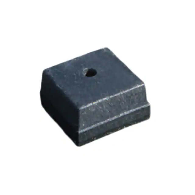
�Package Drawings & Markings
Figure 31: Package Drawing
AS7211
Notes:
1.
2.
3.
4.
5.
Unless otherwise specified, all dimensions are in millimeters.
Tolerances: Angular (± .5°), Two Place Decimal (± .015), Three Place Decimal (± .010)
Contact finish is Au.
This package contains no lead (Pb).
This drawing is subject to change without notice.
AS7211 – 22
ams Preliminary Datasheet, Confidential: [v0-92] 2016–M11–03
�PCB Pad Layout
Suggested PCB pad layout guidelines for the LGA package are show. Flash Gold is
recommended as a surface finish for the landing pads.
Figure 32: Recommended PCB Pad Layout
Unit: mm
0.30
1.10
0.65
4.60
1
4.40
Notes:
1. Unless otherwise specified, all dimensions are in millimeters.
2. Dimensional tolerances are ±0.05mm unless otherwise noted.
3. This drawing is subject to change without notice.
ams Preliminary Datasheet, Confidential: [v0-92] 2016–M11–03
AS7211 – 23
�Mechanical Data
Figure 33: Tape & Reel Information
AS7211 – 24
ams Preliminary Datasheet, Confidential: [v0-92] 2016–M11–03
�Soldering, Manufacturing Process Considerations & Storage
Information
Solder Reflow Profile
The module has been tested and has demonstrated an ability to be reflow soldered
to a PCB substrate. The solder reflow profile describes the expected maximum heat
exposure of components during the solder reflow process of product on a PCB.
Temperature is measured on top of component. The components should be limited
to a maximum of three passes through this solder reflow profile.
Figure 34: Recommended Reflow Soldering Profile
Profile Feature
Reference
Average temperature gradient in preheating
Soak Time
Device
2.5°C/s
tSOAK
2 to 3 minutes
Time above 217°C (T1)
t1
Time above 230°C (T2)
t2
Max 50s
Time above Tpeak - 10°C (T3)
t3
Max 10s
Tpeak
260°C
Peak temperature in reflow
Temperature gradient in cooling
ams Preliminary Datasheet, Confidential: [v0-92] 2016–M11–03
Max 60s
Max - 5°C/s
AS7211 – 25
�Manufacturing Process Considerations
The AS7211 package is compatible with standard reflow no-clean and cleaning
processes including aqueous, solvent or ultrasonic techniques. However, as an
open-aperture device, precautions must be taken to avoid particulate or solvent
contamination as a result of any manufacturing processes, including pick and place,
reflow, cleaning, integration assembly and/or testing. Temporary covering of the
aperture is allowed. To avoid degradation of accuracy or performance in the end
product, care should be taken that any temporary covering and associated
sealants/debris are thoroughly removed prior to any optical testing or final
packaging.
Storage Information
Moisture Sensitivity Optical characteristics of the device can be adversely affected
during the soldering process by the release and vaporization of moisture that has
been previously absorbed into the package. To ensure the package contains the
smallest amount of absorbed moisture possible, each device is baked prior to being
dry packed for shipping. Devices are dry packed in a sealed aluminized envelope
called a moisture-barrier bag with silica gel to protect them from ambient moisture
during shipping, handling, and storage before use.
Shelf Life
The calculated shelf life of the device in an unopened moisture barrier bag is 12
months from the date code on the bag when stored under the following conditions:
• Shelf Life: 12 months
• Ambient Temperature: