MOP-AL202C-BYFY-25E-3IN 数据手册
MOP-AL202C
Parallel Display Specifications
Revision 1.0
�Revision History
Revision
1.0
0.2
0.1
1
Description
Initial Release
Updates as per issue #333
Initial Draft
Author
Clark
Clark
Clark
�Contents
Revision History ............................................................................................................................................ 1
Contents ........................................................................................................................................................ 2
Features ........................................................................................................................................................ 3
Hardware ...................................................................................................................................................... 3
Drawing ..................................................................................................................................................... 3
Interface .................................................................................................................................................... 3
Instructions ................................................................................................................................................... 4
Outline ...................................................................................................................................................... 4
Instruction Table ....................................................................................................................................... 5
Character ROM.......................................................................................................................................... 6
Character RAM .......................................................................................................................................... 7
Timing Characteristics ............................................................................................................................... 7
Initialization............................................................................................................................................... 8
Specifications ................................................................................................................................................ 9
Electrical .................................................................................................................................................... 9
Optical ....................................................................................................................................................... 9
Environmental ........................................................................................................................................... 9
Troubleshooting .......................................................................................................................................... 10
Power ...................................................................................................................................................... 10
Display ..................................................................................................................................................... 10
Communication ....................................................................................................................................... 10
Precautions ............................................................................................................................................. 10
Ordering ...................................................................................................................................................... 11
Part Numbering Scheme ......................................................................................................................... 11
Options .................................................................................................................................................... 11
Contact ........................................................................................................................................................ 11
2
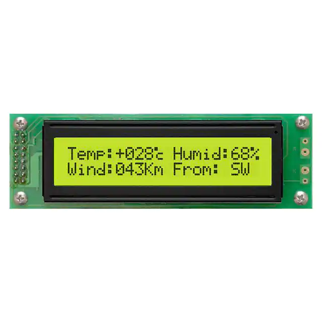
�Features
The Matrix Orbital Parallel display series offers a low cost display solution utilizing an industry standard
communication interface for simple integration into a wide variety of new and existing applications. The
Light Emitting Diode backlight with configurable brightness and voltage controlled contrast allows the
MOP Liquid Crystal Display line to offer a professional display solution with low power impact for any
project. The standard alphanumeric font set also allows up to eight custom characters to be saved in
display Random Access Memory for a custom design touch.
Hardware
2
1
0.40
31.2±0.3
4.0
1.6±0.1
4-Ø3.5
16-Ø1.0
116.0±0.5
Figure 1: MOP-AL202C Mechanical Drawing
Interface
Table 1: Display Control
Pin
1
2
3
4
5
6
15
16
Symbol
VSS
VDD
V0
RS
R/W
CE
LED(+)
LED(-)
Description
Ground
Supply Voltage for Logic
Supply Voltage for LCD (Contrast)
Register Select
Read/Write
Chip Enable
Anode of LED Backlight
Cathode of LED Backlight
Table 2: Parallel Data
Pin
7
8
9
10
11
12
13
14
Symbol
DB0
DB1
DB2
DB3
DB4
DB5
DB6
DB7
Description
*Data bit 0
*Data bit 1
*Data bit 2
*Data bit 3
Data bit 4
Data bit 5
Data bit 6
Data bit 7
*Note: Not used in 4-bit mode
3
0.50
0.05
15
5.55
16
3.20
0.60
0.65
73.50(A.A.)
2.9
2.5
4.0
29.0±0.2
37.0±0.5
9.7±0.5
108.0±0.5
90.8±0.3
83.0(V.A.)
18.6(V.A.)
14.5(MAX.)
9.6
5.0
11.50(A.A.)
P2.54X7=17.78
Drawing
0.05
�Instructions
Outline
The MOP line is controlled using a standard HD44780 compliant controller. The display is enabled by
pulling the Chip Enable (CE) pin high, communication to and from the device is controlled using the
Read/Write (R/W) input, and one of two available 8-bit registers are selected via the Register Select (RS)
line. Using Register Select, either the Instruction Register (IR) or Data Register (DR) is selected by
toggling RS low or high respectively.
While executing from the IR, the display will pull the Most Significant Bit of the data bus, DB7, high.
While this Busy Flag (BF) is set, any instructions sent to the unit will be ignored. The status of this flag
and the current position of the Address Counter (AC) can be obtained by performing a read operation on
the instruction register at any time.
Table 3: Register Selection
RS
0
0
1
1
R/W
0
1
0
1
Operation
IR write as an internal operation (display clear, etc.)
Read busy flag (DB7) and address counter (DB0 to DB6)
Write data to DDRAM or CGRAM (DR to DDRAM or CGRAM)
Read data from DDRAM or CGRAM (DDRAM or CGRAM to DR)
When writing for the DR, one of two locations can be chosen using the AC. The value provided to the AC
when executing a set address command differentiates these locations. The AC is automatically
decremented or incremented after a read or a write.
DDRAM provides eighty bytes of display memory to all displays. Memory outside the bounds of the
display area can be used as general RAM. DDRAM addressing begins at the top left of the display with a
value of 0, addresses then increment from left to right then down once a row is filled.
Table 4: One Line Addressing
Position
DDRAM Address
1
00
2
01
...
...
Table 5: Two Line Addressing
80
4F
Position
DDRAM
Address
1
00
40
2
01
41
...
...
...
40
27
67
Table 6: Four Line Addressing
Position
DDRAM
Address
1
00
40
14
54
2
01
41
15
55
...
...
...
...
...
20
13
53
27
67
CGRAM provides eight custom characters that can be created by writing to CGRAM locations then
displayed using the first eight CGROM character codes, as seen in the character ROM table below.
Characters are sent to the display by performing a write operation on the DR using the correct character
address within CGROM. Instructions are issued by writing to the IR; a complete list is available below.
4
�Instruction Table
Table 7: Parallel Instruction Table
Instruction Code
Instruction
Description
RS
R/W
DB7
DB6
DB5
DB4
DB3
DB2
DB1
DB0
Clear
Display
0
0
0
0
0
0
0
0
0
1
Return
Home
0
0
0
0
0
0
0
0
1
-
Entry Mode
Set
0
0
0
0
0
0
0
1
I/D
SH
Display
ON/OFF
Control
0
0
0
0
0
0
1
D
C
B
Cursor or
Display Shift
0
0
0
0
0
1
S/C
R/L
-
-
Function Set
0
0
0
0
1
DL
N
F
-
-
0
0
0
1
AC5
AC4
AC3
AC2
AC1
AC0
Set CGRAM address in address counter.
0
0
1
AC6
AC5
AC4
AC3
AC2
AC1
AC0
Set DDRAM address in address counter.
0
1
BF
AC6
AC5
AC4
AC3
AC2
AC1
AC0
Read the status of the display controller
through the BF Bit. The contents of
address counter can also be read.
Set CGRAM
Address
Set DDRAM
Address
Read Busy
Flag and
Address
Write Data
to RAM
1
0
D7
D6
D5
D4
D3
D2
D1
D0
Read Data
from RAM
1
1
D7
D6
D5
D4
D3
D2
D1
D0
5
Write “20H” to all DDRAM locations, set
DDRAM address to “00H”, return cursor
to its original position, and set I/D to “1”.
Set DDRAM address to “00H” and return
cursor to its original position if shifted.
The contents of DDRAM are not changed.
Assign cursor moving direction and
enable the shift of entire display. DDRAM
and CRAM addresses are incremented
and cursor moves right when I/D is set to
“1”, the opposite is true when reset to
“0”. Setting SH to “1” causes the entire
display to shift affecting only DDRAM.
Set display (D), cursor (C), and blinking of
cursor (B) on/off control bit. Setting D, C,
or B to “1” will cause the display,
underline cursor, or blinking cursor to
turn on, the opposite is true for reset.
Set cursor moving and display shift
control bit, and the direction, without
changing of DDRAM data. Setting S/L to
“1” will shift the screen horizontally while
the opposite will move the cursor
through all screen positions. Setting R/L
to “1” will shift right immediately. AC
and DDRAM are not altered.
Set interface data length, numbers of
display line and, display font type.
Setting DL to “1” specifies 8-bit mode, “0”
4-bit. Setting N to “1” permits a multiline display, “0” a single. Resetting F to
“0” indicates a 5x8 dot character.
Write data into internal RAM
(DDRAM/CGRAM), location is determined
by the AC. AC and display shift are
adjusted as specified.
Read data from internal RAM
(DDRAM/CGRAM), location is determined
by the AC, set command is recommended
previous to this. Only AC is adjusted.
�Character ROM
The character generator ROM stores up to two hundred fifty-six 5 8 dot character patterns from 8-bit
character codes. The first eight characters are reserved for custom characters saved in CGRAM.
Figure 2: European Character Set
6
�Character RAM
CGRAM allows the creation of up to
eight 5x8 character patterns. Eight
bytes are assigned to each character
address, the least significant five bits of
which represent the five pixel columns.
Pixels are activated by setting the bit in
their position in CGRAM to “1”.
Table 8:Relationship between CGRAM Addresses,
Character Codes (DDRAM Data) and Character Patterns (CGRAM Data)
Each character has eight addresses in
CGRAM corresponding to each of its
eight pixel rows. The highest three bits
represent the character address in
DDRAM. The lowest three bits of this
address represent the row positions
beginning with 0 at the top. The last
row will be logically OR’d with the
cursor when it is active.
Finally, each character can be
referenced in DDRAM and written to
the screen using its eight bit address.
Note: * Indicates no effect.
Timing Characteristics
Table 9: Read and Write Operation Specifications
Item
Enable cycle time
Enable pulse width (high level)
Enable rise/fall time
Address set-up time (RS, R/W to E)
Address hold time
Data set-up time
Data hold time
Figure 3: Write Timing Waveform
7
Symbol
tcycE
PWEH
tEr,tEf
tAS
tAH
tDS
tH
Min
1200
140
-
0
10
40
10
Write
Typ Max
-
-
-
-
25
-
-
-
-
-
-
-
-
-
Read
Min Typ Max Unit
1200 -
ns
-
140
ns
-
-
25
ns
-
-
0
ns
-
-
10
ns
-
-
100
ns
-
-
10
ns
-
-
Conditions: Ta=25℃, VDD=5.0± 0.5V
Figure 4: Read Timing Waveform
�Initialization
Before beginning any application, it is recommended that all display settings be initialized. Below are
algorithms for initializing the display in both 8-bit and 4-bit communication modes.
Before the first wait condition, please allow Vcc to rise to 2.7V then wait 40ms. During the three
function set commands that follow, note that the busy flag cannot be checked; it becomes available in
the last block. The unit will always expect a total of 8 bits to be sent, so note the structure used in four
bit mode. The last initialization block will set the number of lines and character font as specified, turn
the display off, issue the display clear command, and finally set the entry mode as desired.
Figure 5: 8-bit Initialization
Figure 6: 4-bit Initialization
Note: * Indicates do not care condition.
8
�Specifications
Electrical
Table 10: Electrical Characteristics
Item
Supply Voltage For Logic
Supply Voltage For LCD (Contrast)
Input High Voltage
Input Low Voltage
Supply Current (VDD=5V)
Supply Voltage of Red Backlight (42 Die)
Supply Current of Red Backlight (42 Die)
Supply Voltage of Yellow-Green Backlight (42 Die)
Supply Current of Yellow-Green Backlight (42 Die)
Supply Voltage of White Backlight (4 Die)
Supply Current of White Backlight (4 Die)
Symbol
VDD
V0
VIH
VIL
IDD
VLED
ILED
VLED
ILED
VLED
ILED
Min
4.5
-13.5
0.7 VDD
VSS
0.5
3.5
0
3.8
0
3.0
0
Typ
5.0
-
-
-
1.0
3.9
-
4.1
-
3.2
-
Max
5.5
VDD
VDD
0.3 VDD
2.0
4.1
210
4.3
210
3.5
60
Unit
V
V
V
V
mA
V
mA
V
mA
V
mA
Optical
Table 11: Display Characteristics
Item
Number of Characters
Module dimension
View area
Active area
Character size
Character pitch
Dot size
Dot pitch
LCD type
Duty
View direction
θ b
θ f
Dimension
20 Characters x 2 Lines
116.0 x 37.0 x 14.5
83.0 x 18.6
73.50 x 11.50
3.20 x 5.55
3.70 x 5.95
0.60 x 0.65
0.65 x 0.70
STN
1/16
12 o’clock
Unit
-
mm
mm
mm
mm
mm
mm
mm
φ = 180°
θ l
θ r
φ = 90°
φ = 270°
φ = 0°
Figure 7: Viewing Angle Definition
Non-selected
Conition
Selected Conition
Non-selected
Conition
Intensity
10%
Table 12: Viewing Characteristics
Item
View Angle
Contrast Ratio
Response Time
Symbol
(V)θ
(H)φ
CR
T rise
T fall
Min
-20
-30
-
-
-
Typ
-
-
3
-
-
Max
35
30
-
250
250
Unit
deg
deg
-
ms
ms
90%
100%
Tr
Environmental
Table 13: Environmental Specifications
Item
Operating Temp.
Storage Temp.
Note: Maximum 90% non-condensing humidity.
9
Symbol
Top
Tstr
Tf
Figure 8: Display
Time
[positiveResponse
type]
Min
-20
-30
Max
70
80
Unit
℃
℃
�Troubleshooting
Power
For your MOP Display to function correctly, appropriate power must be applied, often as indicated by
the backlight illuminating or a darkening of the character spaces. Please refer to the power diagram
below and reference all voltages to the specifications provided.
Figure 9: Single Supply Configuration
Figure 10: Dual Supply Configuration
Display
If your display is powered successfully, the backlight or contrast should be evident. A lack of text could
be the result of a high contrast voltage, lower V0. Also, ensure the expected DDRAM addresses are
shown by moving the display to the home position.
Communication
When communication of either text or commands is interrupted, check all data and control pins for
continuity. Ensure the display has been initialized correctly before sending information using the
appropriate initialization algorithm. For 4-bit mode ensure D4-D7 are used. Finally, slow down
communication and refer to timing diagrams and specifications for proper control flow.
Precautions
•
•
•
•
•
•
Do not make extra holes on the display, modify its shape, or change the components.
Avoid applying excessive electrical shock to the module.
Do not drop, bend, twist, or disassemble the display.
Avoid operation outside absolute maximum ratings.
Solder only to the I/O terminals provided.
Store in an anti-static container within a clean environment.
10
�Ordering
Part Numbering Scheme
Table 14: Parallel Part Numbering Scheme
MOP
1
-
A
2
L
3
20
4
2
5
C
6
-
B
7
F
8
T
9
W
10
-
2
11
5
12
E
13
-
3
14
I
15
N
16
Options
Table 15: Parallel Part Options
#
1
2
3
Designator
Product Line
Display Type
Screen Type
4
Display Columns
5
Display Rows
6
Display Form Factor
7
IC Package
8
LCD Glass Type
9
Polarizer Style
10
Backlight Colour
11
Viewing Angle
12
Controller
13
Character Set
14
15
16
Input Voltage
Temperature Range
Negative Voltage Generation
Options
MOP: Matrix Orbital Parallel Display
A: Alphanumeric
L: Liquid Crystal Display
8: Eight Character Columns
16: Sixteen Character Columns
20: Twenty Character Columns
24: Twenty-Four Character Columns
40: Forty Character Columns
2: Two Character Rows
4: Four Character Rows
A: A Form Factor
B: B Form Factor
C: C Form Factor
F: F Form Factor
B: Chip on Board
B: STN Positive Blue
F: FFSTN Negative
G: STN Positive Grey
T: FSTN Negative
W: FSTN Positive
Y: STN Positive Yellow
F: Transflective
T: Transmissive
R: Red
Y: Yellow-Green
W: White
1: 6:00
2: 12:00
5: S6A0069 Compatible
E: European
J: Japanese
3: 5.0V
I: Industrial
N: None Provided
Contact
Sales
Support
Online
Phone: 403.229.2737
Phone: 403.204.3750
Purchasing: www.matrixorbital.com
Email: sales@matrixorbital.ca Email: support@matrixorbital.ca Support: www.matrixorbital.ca
11
�