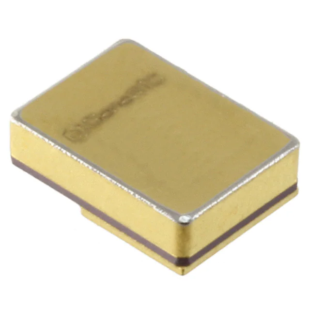
1N8035-GA
High Temperature Silicon Carbide
Power Schottky Diode
VRRM
IF (Tc=25°C)
QC
Features
Package
RoHS Compliant
650 V Schottky rectifier
210 °C maximum operating temperature
Zero reverse recovery charge
Superior surge current capability
Positive temperature coefficient of VF
Temperature independent switching behavior
Lowest figure of merit QC/IF
Available screened to Mil-PRF-19500
=
=
=
650 V
45 A
66 nC
PIN 1
3
1
PIN 3
SMD0.5 / TO – 276 (Hermetic Package)
Advantages
Applications
High temperature operation
Improved circuit efficiency (Lower overall cost)
Low switching losses
Ease of paralleling devices without thermal runaway
Smaller heat sink requirements
Industry’s lowest reverse recovery charge
Industry’s lowest device capacitance
Ideal for output switching of power supplies
Best in class reverse leakage current at operating temperature
Down Hole Oil Drilling
Geothermal Instrumentation
Solenoid Actuators
General Purpose High-Temperature Switching
Amplifiers
Solar Inverters
Switched-Mode Power Supply (SMPS)
Power Factor Correction (PFC)
Maximum Ratings at Tj = 210 °C, unless otherwise specified
Parameter
Repetitive peak reverse voltage
Continuous forward current
Continuous forward current
RMS forward current
Surge non-repetitive forward current, Half Sine
Wave
Non-repetitive peak forward current
2
I t value
Power dissipation
Operating and storage temperature
Symbol
VRRM
IF
IF
IF(RMS)
Conditions
TC = 25 °C
TC ≤ 190 °C
TC ≤ 190 °C
Values
650
45
14.6
26
Unit
V
A
A
A
IF,SM
TC = 25 °C, tP = 10 ms
140
A
IF,max
2
∫i dt
Ptot
Tj , Tstg
TC = 25 °C, tP = 10 µs
650
98
453
-55 to 210
A
2
AS
W
°C
TC = 25 °C, tP = 10 ms
TC = 25 °C
Electrical Characteristics at Tj = 210 °C, unless otherwise specified
Parameter
Symbol
Diode forward voltage
VF
Reverse current
IR
Total capacitive charge
QC
Switching time
ts
Total capacitance
C
Conditions
IF = 15 A, Tj = 25 °C
IF = 15 A, Tj = 210 °C
VR = 650 V, Tj = 25 °C
VR = 650 V, Tj = 210 °C
IF ≤ IF,MAX
VR = 400 V
dIF/dt = 200 A/μs
VR = 400 V
Tj = 210 °C
VR = 1 V, f = 1 MHz, Tj = 25 °C
VR = 400 V, f = 1 MHz, Tj = 25 °C
VR = 650 V, f = 1 MHz, Tj = 25 °C
min.
Values
typ.
1.5
2.2
1
50
66
< 49
1107
103
99
max.
Unit
V
5
200
µA
nC
ns
pF
Thermal Characteristics
Thermal resistance, junction - case
RthJC
0.49
°C/W
0.6
Nm
Mechanical Properties
Mounting torque
Dec 2014
M
http://www.genesicsemi.com/high-temperature-sic/high-temperature-sic-schottky-rectifiers/
Pg 1 of 4
�1N8035-GA
Figure 1: Typical Forward Characteristics
Figure 2: Typical Reverse Characteristics
Figure 3: Power Derating Curve
Figure 4: Current Derating Curves (D = tP/T, tP= 400 µs)
(Considering worst case Zth conditions )
Figure 5: Typical Junction Capacitance vs Reverse Voltage
Characteristics
Figure 6: Typical Capacitive Energy vs Reverse Voltage
Characteristics
Dec 2014
http://www.genesicsemi.com/high-temperature-sic/high-temperature-sic-schottky-rectifiers/
Pg 2 of 4
�1N8035-GA
Figure 7: Current vs Pulse Duration Curves at TC = 190 °C
Figure 8: Transient Thermal Impedance
Package Dimensions:
SMD-0.5/TO-276
PACKAGE OUTLINE
NOTE
1. CONTROLLED DIMENSION IS INCH. DIMENSION IN BRACKET IS MILLIMETER.
2. DIMENSIONS DO NOT INCLUDE END FLASH, MOLD FLASH, MATERIAL PROTRUSIONS
Dec 2014
http://www.genesicsemi.com/high-temperature-sic/high-temperature-sic-schottky-rectifiers/
Pg 3 of 4
�1N8035-GA
Revision History
Date
Revision
Comments
2014/08/26
1
Updated Electrical Characteristics
2012/04/24
0
Initial release
Supersedes
Published by
GeneSiC Semiconductor, Inc.
43670 Trade Center Place Suite 155
Dulles, VA 20166
GeneSiC Semiconductor, Inc. reserves right to make changes to the product specifications and data in this document without notice.
GeneSiC disclaims all and any warranty and liability arising out of use or application of any product. No license, express or implied to any
intellectual property rights is granted by this document.
Unless otherwise expressly indicated, GeneSiC products are not designed, tested or authorized for use in life-saving, medical, aircraft
navigation, communication, air traffic control and weapons systems, nor in applications where their failure may result in death, personal
injury and/or property damage.
Dec 2014
http://www.genesicsemi.com/high-temperature-sic/high-temperature-sic-schottky-rectifiers/
Pg 4 of 4
�
1N8035-GA
SPICE Model Parameters
Copy the following code into a SPICE software program for simulation of the 1N8035-GA device.
*
MODEL OF GeneSiC Semiconductor Inc.
*
*
$Revision:
1.0
$
*
$Date:
05-SEP-2013
$
*
*
GeneSiC Semiconductor Inc.
*
43670 Trade Center Place Ste. 155
*
Dulles, VA 20166
*
http://www.genesicsemi.com/index.php/hit-sic/schottky
*
*
COPYRIGHT (C) 2013 GeneSiC Semiconductor Inc.
*
ALL RIGHTS RESERVED
*
* These models are provided "AS IS, WHERE IS, AND WITH NO WARRANTY
* OF ANY KIND EITHER EXPRESSED OR IMPLIED, INCLUDING BUT NOT LIMITED
* TO ANY IMPLIED WARRANTIES OF MERCHANTABILITY AND FITNESS FOR A
* PARTICULAR PURPOSE."
* Models accurate up to 2 times rated drain current.
*
* Start of 1N8035-GA SPICE Model
*
.SUBCKT 1N8035 ANODE KATHODE
D1 ANODE KATHODE 1N8035_25C; Call the Schottky Diode Model
D2 ANODE KATHODE 1N8035_PIN; Call the PiN Diode Model
.MODEL 1N8035_25C D
+ IS
8.46E-17
RS
0.0319
+ N
1
IKF
1000
+ EG
1.2
XTI
3
+ TRS1
0.0038
TRS2
3.00E-05
+ CJO
1.26E-09
VJ
0.438
+ M
1.5278
FC
0.5
+ TT
1.00E-10
BV
650
+ IBV
1.00E-03
VPK
650
+ IAVE
20
TYPE
SiC_Schottky
+ MFG
GeneSiC_Semiconductor
.MODEL 1N8035_PIN D
+ IS
2.77E-10
RS
0.086693
+ N
3.3505
IKF
3.67E-06
+ EG
3.23
XTI
-10
+ FC
0.5
TT
0
+ BV
650
IBV
1.00E-03
+ VPK
650
IAVE
20
+ TYPE
SiC_PiN
.ENDS
*
* End of 1N8035-GA SPICE Model
Dec 2014
http://www.genesicsemi.com/high-temperature-sic/high-temperature-sic-schottky-rectifiers/
Page 1 of 1
�Mouser Electronics
Authorized Distributor
Click to View Pricing, Inventory, Delivery & Lifecycle Information:
GeneSiC Semiconductor:
1N8035-GA
�
很抱歉,暂时无法提供与“1N8035-GA”相匹配的价格&库存,您可以联系我们找货
免费人工找货