����
SLG59M1470V
9.8 mΩ, Nanopower Mobile
6 A Load Switch with Discharge
General Description
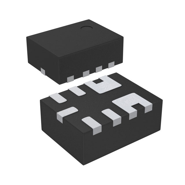
Pin Configuration
The SLG59M1470V is a 9.8 mΩ, 6 A single-channel load
switch that is able to switch 0.85 V to 3.3 V power rails. The
product is packaged in an ultra-small 1.5 x 2.0 mm package.
ON
1
D
2
D
3
D
4
Features
• 1.5 x 2.0 mm FC-TDFN 9L package (2 fused pins for drain
and 2 fused pins for source)
• Logic level ON pin capable of supporting 0.85 V CMOS
Logic
• Discharged Load when off
• Fast Turn On time
• Low RDSON while supporting 6 A
• Pb-Free / Halogen-Free / RoHS compliant
• Operating Temperature: -40 °C to 85 °C
• Operating Voltage: 3.0 V to 5.25 V
9
SLG59M1470V
VDD
8
GND
7
S
6
S
5
S
9-pin FC-TDFN
(Top View)
Applications
•
•
•
•
Watch Power Rail Switching
Tablet Power Rail Switching
Smartphone Power Rail Switching
Notebook Power Rail Switching
Block Diagram
6.0 A @ 9.8 mΩ
D
S
RDISCHRG
180 Ω
VDD
+3.0 V to 5.25 V
ON
Datasheet
CFR0011-120-01
Input
Circuit
Revision 1.28
Page 1 of 12
2-Feb-2022
©2022 Renesas Electronics Corporation
�����
SLG59M1470V
9.8 mΩ, Nanopower Mobile
6 A Load Switch with Discharge
Pin Description
Pin #
Pin Name
Type
Pin Description
1
VDD
PWR
VDD power for load switch control (3.0 V to 5.25 V)
2
D
MOSFET Drain of Power MOSFET
3
D
MOSFET Drain of Power MOSFET (fused with pin 4)
4
D
MOSFET Drain of Power MOSFET (fused with pin 3)
5
S
MOSFET Source of Power MOSFET (fused with pin 6)
6
S
MOSFET Source of Power MOSFET (fused with pin 5)
7
S
MOSFET Source of Power MOSFET
8
GND
GND
Ground
9
ON
Input
Turns MOSFET ON (4 MΩ pull down resistor)
CMOS input with ON_VIL < 0.2 V, ON_VIH > 0.85 V
Ordering Information
Part Number
Type
Production Flow
SLG59M1470V
FC-TDFN 9L
Industrial, -40 °C to 85 °C
SLG59M1470VTR
FC-TDFN 9L (Tape and Reel)
Industrial, -40 °C to 85 °C
SLG59M1470V RDSON
SLG5AP1471V
20
18
16
Rdson (mё)
14
12
10
8
6
4
2
0
1.5
2
2.5
3
3.5
4
Vdd - Vd (V)
Datasheet
CFR0011-120-01
Revision 1.28
Page 2 of 12
2-Feb-2022
©2022 Renesas Electronics Corporation
�����
SLG59M1470V
9.8 mΩ, Nanopower Mobile
6 A Load Switch with Discharge
Absolute Maximum Ratings
Parameter
VDD
TS
ESDHBM
Description
Conditions
Min.
Typ.
Max.
Unit
--
--
7
V
-65
--
150
°C
2000
--
--
V
Power Supply
Storage Temperature
ESD Protection
MSL
Moisture Sensitivity Level
WDIS
Package Power Dissipation
Human Body Model
1
MOSFET IDSPK Peak Current from Drain to Source For no more than 1 ms with 1% duty cycle
--
--
1.0
W
--
--
9
A
Note: Stresses greater than those listed under “Absolute Maximum Ratings” may cause permanent damage to the device. This is a stress rating
only and functional operation of the device at these or any other conditions above those indicated in the operational sections of this
specification is not implied. Exposure to absolute maximum rating conditions for extended periods may affect reliability.
Electrical Characteristics
TA = -40 °C to 85 °C (unless otherwise noted)
Parameter
VDD
IDD
RDSON
RDSON
RDSON
Description
Power Supply Voltage
Power Supply Current (PIN 1)
ON Resistance
ON Resistance
ON Resistance
MOSFET IDS Current from D to S
VD
Datasheet
CFR0011-120-01
Conditions
-40 °C to 85 °C
1
Min.
Typ.
Max.
Unit
3.0
--
5.25
V
when OFF, TA = 25 °C
--
30
60
nA
when ON, No load,
ON = VDD, TA = 25 °C
--
35
70
nA
when OFF, TA = 70 °C
--
100
900
nA
when ON, No load,
ON = VDD, TA = 70 °C
--
200
900
nA
TA = 25 °C; IDS = 300 mA, VDD - VD = 1.5 V
--
16.2
18.6
mΩ
TA = 25 °C; IDS = 300 mA, VDD - VD = 2.0 V
--
11.5
13.2
mΩ
TA = 25 °C; IDS = 300 mA, VDD - VD = 2.5 V
--
9.5
10.9
mΩ
TA = 25 °C; IDS = 300 mA, VDD - VD = 3.0 V
--
8.5
9.8
mΩ
TA = 25 °C; IDS = 300 mA, VDD - VD = 3.5 V
--
7.9
9.1
mΩ
TA = 25 °C; IDS = 300 mA, VDD - VD = 4.0 V
--
7.4
8.5
mΩ
TA = 70 °C; IDS = 300 mA, VDD - VD = 1.5 V
--
19.2
22.1
mΩ
TA = 70 °C; IDS = 300 mA, VDD - VD = 2.0 V
--
14.1
16.2
mΩ
TA = 70 °C; IDS = 300 mA, VDD - VD = 2.5 V
--
11.7
13.5
mΩ
TA = 70 °C; IDS = 300 mA, VDD - VD = 3.0 V
--
10.5
12.1
mΩ
TA = 70 °C; IDS = 300 mA, VDD - VD = 3.5 V
--
9.7
11.2
mΩ
TA = 70 °C; IDS = 300 mA, VDD - VD = 4.0 V
--
9.2
10.6
mΩ
TA = 85 °C; IDS = 300 mA, VDD - VD = 1.5 V
--
24.96
28.73
mΩ
TA = 85 °C; IDS = 300 mA, VDD - VD = 2.0 V
--
18.33
21.06
mΩ
TA = 85 °C; IDS = 300 mA, VDD - VD = 2.5 V
--
15.21
17.55
mΩ
TA = 85 °C; IDS = 300 mA, VDD - VD = 3.0 V
--
13.65
15.73
mΩ
TA = 85 °C; IDS = 300 mA, VDD - VD = 3.5 V
--
12.61
14.56
mΩ
TA = 85 °C; IDS = 300 mA, VDD - VD = 4.0 V
--
11.96
13.78
mΩ
Continuous
--
--
6
A
--
VDD
- 1.5
V
Drain Voltage
0.85
Revision 1.28
Page 3 of 12
2-Feb-2022
©2022 Renesas Electronics Corporation
�����
SLG59M1470V
9.8 mΩ, Nanopower Mobile
6 A Load Switch with Discharge
Electrical Characteristics (continued)
TA = -40 °C to 85 °C (unless otherwise noted)
Parameter
Description
Min.
Typ.
Max.
Unit
50% ON to 90% VS, VDD = 5.25 V,
VD = 1.0 V, CLOAD = 10 µF, RLOAD = 20 Ω
7
9
12
µs
50% ON to 90% VS, VDD = 5.25 V,
VD = 1.0 V, CLOAD = 2 µF, RLOAD = 20 Ω
8
10
12
µs
50% ON to 90% VS, VDD = 5 V, VD = 1.0 V,
CLOAD = 2 x (50 µF + 2.2 µH Inductor) 2
30
42
50
µs
10% VS to 90% VS, VDD = 5.25 V,
VD = 1.0 V, CLOAD = 10 µF, RLOAD = 20 Ω
130
160
190
V/ms
10% VS to 90% VS, VDD = 5.25 V,
VD = 1.0 V, CLOAD = 2 µF, RLOAD = 20 Ω
150
176
200
V/ms
10% VS to 90% VS, VDD = 5 V,
VD = 1.0 V, RLOAD = 20 Ω,
CLOAD = 2 x (50 µF + 2.2 µH Inductor) 2
20
26
35
V/ms
CLOAD connected from S to GND
--
--
10
µF
Discharge Resistance
100
180
300
Ω
ON_VIH
High Input Voltage on ON pin
0.85
--
VDD
V
ON_VIL
Low Input Voltage on ON pin
TTotal_ON
Conditions
Total Turn On Time
VS(SR)
VS Slew Rate
CLOAD
Output Load Capacitance
RDISCHRG
TOFF_Delay
TFALL
-0.3
0
0.2
V
OFF Delay Time
50% ON to VS Fall Start ↓, VDD = 5.25 V,
VD = 1.0 V, RLOAD = 20 Ω, no CLOAD
--
--
60
µs
VS Fall Time
90% VS to 10% VS, VDD = 5.25 V,
VD = 1.0 V, RLOAD = 20 Ω, no CLOAD
--
15
--
µs
Notes:
1. Guaranteed by design and characterization
2. See Application Diagram below regarding CLOAD = 2 x (50 µF + 2.2 µH).
Application Diagram (Source loading > 10 µF)
2.2 µH
S
S
S
1 µF
50 µF
2.2 µH
50 µF
Capacitive loads > 10 µF directly on the S pin may result in nonlinear output ramping. In cases
where > 10 µF load capacitance is required, we recommend decoupling the load(s) with 2.2 µH
inductors while putting a 1 µF capacitor on S as shown above in order to guarantee linear
ramping and inrush current limiting.
Datasheet
CFR0011-120-01
Revision 1.28
Page 4 of 12
2-Feb-2022
©2022 Renesas Electronics Corporation
�����
SLG59M1470V
9.8 mΩ, Nanopower Mobile
6 A Load Switch with Discharge
TTotal_ON, TON_Delay and Slew Rate Measurement
ON*
50% ON
50% ON
TOFF_Delay
90% VS
VS
90% VS
TON_Delay
10% VS
10% VS
VS(SR) (V/ms)
TFALL
TTotal_ON
*Rise and Fall Times of the ON Signal are 100 ns
Datasheet
CFR0011-120-01
Revision 1.28
Page 5 of 12
2-Feb-2022
©2022 Renesas Electronics Corporation
�����
SLG59M1470V
9.8 mΩ, Nanopower Mobile
6 A Load Switch with Discharge
Layout Guidelines:
1. The VDD pin needs a 0.1 µF and 10 µF external capacitors to smooth pulses from the power supply. Locate these capacitors
as close as possible to the SLG59M1470V's PIN1.
2. Since the D and S pins dissipate most of the heat generated during high-load current operation, it is highly recommended to
make power traces as short, direct, and wide as possible. A good practice is to make power traces with absolute minimum
widths of 15 mils (0.381 mm) per Ampere. A representative layout, shown in Figure 1, illustrates proper techniques for heat to
transfer as efficiently as possible out of the device;
3. To minimize the effects of parasitic trace inductance on normal operation, it is recommended to connect input CIN and output
CLOAD low-ESR capacitors as close as possible to the SLG59M1470V's D and S pins;
4. The GND pin should be connected to system analog or power ground plane.
5. 2 oz. copper is recommended for high current operation.
SLG59M1470V Evaluation Board:
А GreenFET Evaluation Board for SLG59M1470V is designed according to the statements above and is illustrated on Figure 1.
Please note that evaluation board has D_Sense and S_Sense pads. They cannot carry high currents and dedicated only for
RDSON evaluation.
Please solder your SLG59M1470V here
Figure 1. SLG59M1470V Evaluation Board
Datasheet
CFR0011-120-01
Revision 1.28
Page 6 of 12
2-Feb-2022
©2022 Renesas Electronics Corporation
�����
SLG59M1470V
9.8 mΩ, Nanopower Mobile
6 A Load Switch with Discharge
1
1
VDD
C2
1
2
3
4
5
VDD CAP2
GND CAP1
ON1
S2
ON2
S1
D1
D2
C1
10
9
8
7
6
CAP/RILIM
ON
D_Sense1
1
1
2
3
1
2
3
4
U1
VDD
ON
D
D
C3
C4
R_Array
1
3
5
7
9
8
7
6
5
GND
PG
S
S
1
3
5
7
9
S_Sense1
1
C5
R1
C6
2
4
6
8
10
R2
R3
R4
C7
100n
2
4
6
8
10
9
1
2
3
4
D_Sense2
1
U2
ON
VDD
D
D
D
8
7
6
5
GND
CAP
S
S
S_Sense2
1
C8
100n
1
2
3
4
D_Sense3
1
U3
ON
VDD
D
D
8
7
6
5
GND
CAP
S
S
S_Sense3
1
C9
100n
9
1
2
3
4
D_Sense4
1
1
2
3
4
D_Sense5
1
1
2
D_Sense6
1
U4
ON
VDD
D
D
D
8
7
6
5
GND
S
S
S
U5
ON
VIN
VIN
VIN
U6
ON
D
8
7
6
5
GND
VOUT
VOUT
VOUT
GND
S
S_Sense4
1
S_Sense5
1
4
3
D/VIN
D/VIN
1
1
1
1
S_Sense6
1
S/VOUT S/VOUT
Figure 2. SLG59M1470V Evaluation Board Connection Circuit
Datasheet
CFR0011-120-01
Revision 1.28
Page 7 of 12
2-Feb-2022
©2022 Renesas Electronics Corporation
�����
SLG59M1470V
9.8 mΩ, Nanopower Mobile
6 A Load Switch with Discharge
Basic Test Setup and Connections
Figure 3. SLG59M1470V Evaluation Board Connection Circuit
EVB Configuration
1. Connect oscilloscope probes to D/VIN, S/VOUT, ON, etc.;
2. Turn on Power Supply 1 and set desired VDD from 3 V…5.25 V range;
3. Turn on Power Supply 2 and set desired VD from 0.85 V…VDD - 1.5 V range;
4. Toggle the ON signal High or Low to observe SLG59M1470V operation.
SLG59M1470V Layout Suggestion
2300
700
210
800
800
9
1
Exposed Pad
210
Recommended Land Pattern
1410
190
8
610
Unit: µm
1000
Datasheet
CFR0011-120-01
Revision 1.28
Page 8 of 12
2-Feb-2022
©2022 Renesas Electronics Corporation
�����
SLG59M1470V
9.8 mΩ, Nanopower Mobile
6 A Load Switch with Discharge
Package Top Marking System Definition
Date Code + Revision
Pin 1 Identifier
JZA
DDR
LL
Part Code + Assembly Site
Lot Traceability
JZ - Part Code1
A - Assembly Site Code Field2
DD - Date Code Field1
R - Part Revision Code Field2
LL - Lot Traceability Field1
Note 1: Each character in code field can be alphanumeric A-Z and 0-9
Note 2: Character in code field can be alphabetic A-Z
Datasheet
CFR0011-120-01
Revision 1.28
Page 9 of 12
2-Feb-2022
©2022 Renesas Electronics Corporation
�����
SLG59M1470V
9.8 mΩ, Nanopower Mobile
6 A Load Switch with Discharge
Package Drawing and Dimensions
9 Lead TDFN FC Package 1.5 x 2.0 mm (Fused Lead)
JEDEC MO-252, Variation W2015D
Datasheet
CFR0011-120-01
Revision 1.28
Page 10 of 12
2-Feb-2022
©2022 Renesas Electronics Corporation
�����
SLG59M1470V
9.8 mΩ, Nanopower Mobile
6 A Load Switch with Discharge
Tape and Reel Specifications
Max Units
Leader (min)
Nominal
Reel &
Package # of
Package Size
Hub Size
Length
Type
Pins
per Reel per Box
Pockets
[mm]
[mm]
[mm]
TDFN 9L
FC Green
9
1.5 x 2.0 x 0.75
3000
3000
178 / 60
100
400
Trailer (min)
Pockets
Length
[mm]
Tape
Width
[mm]
100
400
8
Part
Pitch
[mm]
4
Carrier Tape Drawing and Dimensions
Package
Type
Pocket BTM Pocket BTM
Length
Width
TDFN 9L
FC Green
Pocket
Depth
Index Hole
Pitch
Pocket
Pitch
Index Hole
Diameter
Index Hole Index Hole
to Tape
to Pocket Tape Width
Edge
Center
A0
B0
K0
P0
P1
D0
E
F
W
1.68
2.18
0.9
4
4
1.5
1.75
3.5
8
P0
D0
E
Y
W
F
Section Y-Y
B0
CL
K0
Y
P1
A0
Refer to EIA-481 specification
Recommended Reflow Soldering Profile
Please see IPC/JEDEC J-STD-020: latest revision for reflow profile based on package volume of 2.25 mm3 (nominal). More
information can be found at www.jedec.org.
Datasheet
CFR0011-120-01
Revision 1.28
Page 11 of 12
2-Feb-2022
©2022 Renesas Electronics Corporation
�����
SLG59M1470V
9.8 mΩ, Nanopower Mobile
6 A Load Switch with Discharge
Revision History
Date
Version
2/2/2022
1.28
Updated Company name and logo
Fixed typos
1/29/2019
1.27
Updated style and formatting
Added Layout Guidelines
Fixed typos
10/5/2016
1.26
Updated TTotal_ON, VOUT(SR), TOFF_Delay, TFALL specs
Updated Application Diagram Notes
Updated Formating and Parameter Names for clarity
4/26/2016
1.25
Added MSL 1
Added Part Code Marking Information
9/04/2015
1.24
Fixed TA conditions in Electrical Characteristics
Datasheet
CFR0011-120-01
Change
Revision 1.28
Page 12 of 12
2-Feb-2022
©2022 Renesas Electronics Corporation
�IMPORTANT NOTICE AND DISCLAIMER
RENESAS ELECTRONICS CORPORATION AND ITS SUBSIDIARIES (“RENESAS”) PROVIDES TECHNICAL
SPECIFICATIONS AND RELIABILITY DATA (INCLUDING DATASHEETS), DESIGN RESOURCES (INCLUDING
REFERENCE DESIGNS), APPLICATION OR OTHER DESIGN ADVICE, WEB TOOLS, SAFETY INFORMATION, AND
OTHER RESOURCES “AS IS” AND WITH ALL FAULTS, AND DISCLAIMS ALL WARRANTIES, EXPRESS OR IMPLIED,
INCLUDING, WITHOUT LIMITATION, ANY IMPLIED WARRANTIES OF MERCHANTABILITY, FITNESS FOR A
PARTICULAR PURPOSE, OR NON-INFRINGEMENT OF THIRD PARTY INTELLECTUAL PROPERTY RIGHTS.
These resources are intended for developers skilled in the art designing with Renesas products. You are solely responsible
for (1) selecting the appropriate products for your application, (2) designing, validating, and testing your application, and (3)
ensuring your application meets applicable standards, and any other safety, security, or other requirements. These
resources are subject to change without notice. Renesas grants you permission to use these resources only for
development of an application that uses Renesas products. Other reproduction or use of these resources is strictly
prohibited. No license is granted to any other Renesas intellectual property or to any third party intellectual property.
Renesas disclaims responsibility for, and you will fully indemnify Renesas and its representatives against, any claims,
damages, costs, losses, or liabilities arising out of your use of these resources. Renesas' products are provided only subject
to Renesas' Terms and Conditions of Sale or other applicable terms agreed to in writing. No use of any Renesas resources
expands or otherwise alters any applicable warranties or warranty disclaimers for these products.
(Rev.1.0 Mar 2020)
Corporate Headquarters
Contact Information
TOYOSU FORESIA, 3-2-24 Toyosu,
Koto-ku, Tokyo 135-0061, Japan
www.renesas.com
For further information on a product, technology, the most
up-to-date version of a document, or your nearest sales
office, please visit:
www.renesas.com/contact/
Trademarks
Renesas and the Renesas logo are trademarks of Renesas
Electronics Corporation. All trademarks and registered
trademarks are the property of their respective owners.
© 2021 Renesas Electronics Corporation. All rights reserved.
�