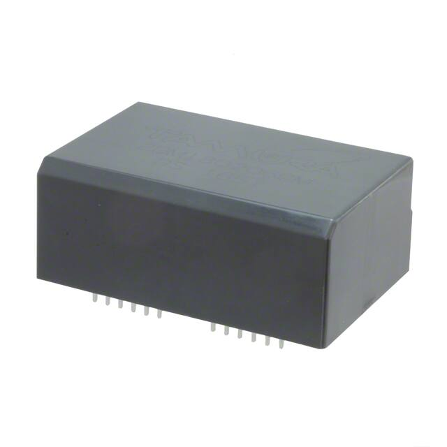
2DM150806CM
Datasheet
■Absolute Maximum Ratings
Item
Symbol
Min
Max
Unit
VIN
-0.3
28
Vdc
VINMIN
13
-
Vdc
Input-side signal voltage
VSG
-0.3
5.2
V
Input-side signal maximum current
ISG
-
5
mA
DESAT pin input voltage
VDESAT
-0.3
VOUTH+0.3
V
CLAMP pin input voltage
VCLAMP VOUTL-0.3 VOUTH+0.3
V
OUT pin output current(peak)
IOUTPEAK
-
18
A
Guaranteed by design
Output power for DC/DC converter
POUT
-
3
W
By one circuit
Switching frequency
FSW
-
200
kHz
Operating temperature range
TOP
-30
85
℃
Operating humidity
RHOP
20
95
%RH
Storage temperature range
TSTG
-30
100
℃
Storage humidity
RHSTG
5
95
%RH
Item
Symbol
Min
Max
Unit
Input voltage range for DC/DC converter
VIN
13.5
26.4
Vdc
Driver circuit number
N
-
2
-
Logic high level input voltage
VSGH
2
5
V
INA, INB ,XRST
Logic low level input voltage
VSGL
0
0.8
V
INA, INB ,XRST
ISG
20
-
mA
INA, INB, XRST, VSG=5V
Maximum gate drive capability(200kHz)
QMAX
-
600
nC
TOP=55℃ Reference value
Maximum gate drive capability(50kHz)
QMAX
-
2400
nC
TOP=55℃ Reference value
Minimum input pulse width
tINMSK
-
60
ns
Input voltage for DC/DC converter
Minimum operating input voltage for DC/DC converter
Conditions・Note
Between Vin(+) to Vin(-)
INA, INB, XRST, RDY, FLT
RDY, FLT
See the derating curve
No condensation
No condensation
■Recommended Operating Conditons
Source current of control signal
TAMURA CORPORATION
1 / 15
Conditions・Note
Rated Input Voltage:24V
Rev.B May, 2017
�2DM150806CM
Datasheet
■Electrical Specification (Ta=25℃)
DC/DC converter block
Item
Start-up voltage
Efficiency
Standby power
Conditions・Note
Symbol
Min
Typ
Max
Unit
VSTART
-
11.5
12.5
V
Effi
69
74
-
%
Rated Input Voltage, IOUTAVE(CH1,2):100mA
PSTBY
-
0.7
1
W
Rated Input Voltage, No load
14.5
15.5
16.5
V
IOUTAVE(CH1) = IOUTAVE(CH2) = 10-130mA
14.5
15.5
17.0
V
IOUTAVE(CH1) = IOUTAVE(CH2) = 0-10mA
IOUTAVE(CH1) = IOUTAVE(CH2) = 0-130mA
Output voltage(Hgih)
V1+,V2+
Output voltage(Low)
V1-,V2-
-9
-8
-7
V
V5VDC
4.8
5.0
5.2
V
Output Voltage(High)(Load imbalance) V1+,V2+
-
-
22
V
Output Voltage(Low)(Load imbalance) V1-,V2-
-12
-
-
V
Symbol
Min
Typ
Max
Unit
Logic high level input voltage
VSGH
2
-
Logic low level input voltage
VSGL
0
-
0.8
V
INA, INB ,XRST
Logic pull-down resistance
RSGD
-
270
-
Ω
INA, INB ,XRST
Logic pull-up resistance
RSGU
-
5100
-
Ω
RDY, FLT
Logic input mask time
tINMSK
-
-
60
ns
INA, INB
tXRSTMIN
800
-
-
ns
Output voltage(5VDC)
IOUTAVE(CH1):100mA,IOUTAVE(CH2):0mA
or IOUTAVE(CH1):0mA,IOUTAVE(CH2):100mA
Gate drive block
Item
Conditions・Note
Logic
Minimum XRST pulse width
V5VDC V
TAMURA CORPORATION
2 / 15
INA, INB ,XRST
Rev.B May, 2017
�2DM150806CM
Datasheet
■Electrical Specification - Continued (Ta=25℃)
Gate drive block - continued
Item
Symbol
Min
Typ
Max
Unit
Conditions・Note
Output pin voltage(Hgih)
VOUTH
-
VDCDCOH-0.5
-
V
No load
Output pin voltage(Low)
VOUTL
-
VDCDCOL+0.5
-
V
No load, Miller clamp pin no used
-
VDCDCOL+0.1
-
V
No load, Miller clamp pin used
Output
OUT ON resistance(Source)
RONH
-
-
50
mΩ
Guaranteed by design
OUT ON resistance(Sink)
RONL
-
-
50
mΩ
Guaranteed by design
CLAMP ON resistance
RONPRO
0.2
0.5
0.9
Ω
ICLAMP=40mA
Low level CLAMP current
ICLAMPL
3
4.5
-
A
Guaranteed by design
CLAMP ON threshold voltage
VCLPON VOUTL+1.8 VOUTL+2 VOUTL+2.2
V
Guaranteed by design
Turn ON time
tPON
55
80
105
ns
Turn OFF time
tPOFF
55
80
105
ns
Symbol
Min
Typ
Max
Unit
Overload protection
-
6
-
-
W
Auto recovery
Overheat protection
-
120
-
150
℃
Internal temperature
Symbol
Min
Typ
Max
Unit
5VDC UVLO OFF voltage
VUVLO5VH
3.35
3.50
3.65
V
Guaranteed by design
5VDC UVLO ON voltage
VUVLO5VL
3.25
3.40
3.55
V
Guaranteed by design
TUVLO5VMSK
1.0
2.5
5.0
us
Guaranteed by design
OUT(H) UVLO OFF voltage
VUVLOOHH
11.3
12.3
13.3
V
Guaranteed by design
OUT(H) UVLO ON voltage
VUVLOOHL
10.3
11.3
12.3
V
Guaranteed by design
OUT(H) UVLO mask time
TUVLOOHMSK
1.0
2.0
3.0
us
Guaranteed by design
DESAT source current
IDESAT
450
500
550
uA
DESAT threshold voltage
VDESAT
8.5
9
9.5
V
DESAT filter time
tDESATFIL
0.16
0.25
0.34
us
Guaranteed by design
DESAT delay time(OUT)
tDESATOUT
0.31
0.38
0.45
us
Guaranteed by design
DESAT delay time(FLT)
tDESATFLT
0.34
0.42
0.5
us
Guaranteed by design
DESAT low voltage
VDESATL
-
0.1
0.22
V
IDESAT=1mA
DESAT leading edge blanking
tDESTLEB
0.28
0.4
0.52
us
Guaranteed by design
RDY output low voltage
VRDYL
-
0.08
0.15
V
IRDY=5mA
FLT output low voltage
VFLTL
-
0.08
0.15
V
IFLT=5mA
Delay time
■Protection
DC/DC converter block
Item
Conditions・Note
Gate drive block
Item
5VDC UVLO UVLO mask time
TAMURA CORPORATION
3 / 15
Conditions・Note
Rev.B May, 2017
�2DM150806CM
Datasheet
■Insulation
Item
Specification
Conditions・Note
Between Input-Output
Dielectric withstand voltage
AC2500V
1min, Cutoff 2mA
Test dielectric withstand voltage
AC2500V
1sec, Cutoff 2mA
Insulation resistance
100MΩ or more
DC500V
Minimum clearance distances
6mm
Minimum creepage distances
6mm
Between Ch1-Ch2
Dielectric withstand voltage
AC2500V
1min, Cutoff 2mA
Test dielectric withstand voltage
AC2500V
1sec, Cutoff 2mA
Insulation resistance
100MΩ or more
DC500V
Minimum clearance distances
6mm
Minimum creepage distances
6mm
■Ambient Temperature Derating Curve
Reduce the input power according to the following temperature derating table.
Input Power[W]
10
5
2.5
0
10
20
30
40
50
60
70
Operating Temperature Range[℃]
TAMURA CORPORATION
4 / 15
80
90
100
Rev.B May, 2017
�2DM150806CM
Datasheet
■Measure Circuit
【DC/DC converter】
DC/DC Converter Brock
V1+
Vin(+)
A1
A2
V2
V1
E1
V1o
Vin(-)
RL1
V4
E1
: DC power supply
A1-4
: Ammeter Class 0.5
RL1-3
: Electronic load
V1-6
: Voltmeter Class 0.5
E1
: DC power supply
A1
: Ammeter Class 0.5
OS1
: Oscilloscope
P1-4
: Probe
Rg
: 4Ω
Ra
: 47kΩ
rg
: 1Ω
cg
: 100nF
V1A4
5VDC
V2+
A3
V3
RL3
V2o
V6
RL2
V5
S_GND
V2-
【Gate drive】
1 Vin(+)
2 N.C.
3 N.C.
4 Vin(-)
5 N.C.
6 N.C.
7 XRST1
8 FLT1
9 RDY1
10 INB1
11 INA1
12 GND1
13 N.C.
14 XRST2
15 FLT2
16 RDY2
17 INB2
18 INA2
19 GND2
A1
Controller/Monitor
E1
Device
equivalent
circuit
DESAT1
CLAMP1
OUT1
OUT1
COM1
COM1
DESAT2
CLAMP2
OUT2
OUT2
COM2
COM2
34
33
32
31
30
29
20
21
22
23
24
25
rg
Ra
Rg
cg
P3
rg
Ra
Rg
cg
P4
OS1
P2
P1
【Rising waveform/Falling waveform 】
tPON
tPOFF
ON
INA
OUT
TAMURA CORPORATION
5 / 15
Rev.B May, 2017
�2DM150806CM
Datasheet
■Block Diagram
VIN(+)
GND1
5.1k
5.1k
1u
270
270
DESAT detection
DESAT1
Miller Clamp
CLAMP1
OUT1
COM1
270
VCC
60u
LOGIC
FLT1
RDY1
XRST1
INB1
INA1
Gate Drive Ch1
LOGIC
VIN(-)
V2+
Overheat
protection
GND
V2o
V2-
Overload
protection
V1+
5V
DC/DC converter
S_GND
V1o
V1-
Gate Drive Ch2
GND2
5.1k
1u
270
270
LOGIC
5.1k
LOGIC
FLT2
RDY2
XRST2
INB2
INA2
DESAT detection
DESAT2
Miller Clamp
CLAMP2
OUT2
COM2
270
TAMURA CORPORATION
6 / 15
Rev.B May, 2017
�2DM150806CM
Datasheet
■Pin Connection
See the next section for details of pin functions
Input side
Pin No.
1
Name
CH
Explanation of pins
Vin(+) Common Power supply pin for DC/DC converter(+)
2
N.C.
-
Unused pin *Don't connect with other circuits.
3
N.C.
-
Unused pin *Don't connect with other circuits.
4
Vin(-) Common Power supply pin for DC/DC converter(-)
5
N.C.
-
Unused pin *Don't connect with other circuits.
6
N.C.
-
Unused pin *Don't connect with other circuits.
7
XRST1
1
Reset input pin
8
FLT1
1
Fault output pin
9
RDY1
1
Ready output pin
10
INB1
1
Opposite driver's control input pin
11
INA1
1
Control input pin
12
GND1
1
Ground pin for control circuit
13
N.C.
-
Unused pin *Don't connect with other circuits.
14
XRST2
2
Reset input pin
15
FLT2
2
Fault output pin
16
RDY2
2
Ready output pin
17
INB2
2
Opposite driver's control input pin
18
INA2
2
Control input pin
19
GND2
2
Ground pin for control circuit
Output side
Pin No.
Name
CH
Explanation of pins
20
DESAT2
2
Desaturation protection pin
21
CLAMP2
2
Miller clamp pin
22
OUT2
2
Gate drive pin
23
OUT2
2
Gate drive pin
24
COM2
2
Common pin
25
COM2
2
Common pin
26
NONE
-
None
27
NONE
-
None
28
NONE
-
None
29
COM1
1
Common pin
30
COM1
1
Common pin
31
OUT1
1
Gate drive pin
32
OUT1
1
Gate drive pin
33
CLAMP1
1
Miller clamp pin
34
DESAT1
1
Desaturation protection pin
TAMURA CORPORATION
7 / 15
Rev.B May, 2017
�2DM150806CM
Datasheet
■Terminal Function
・Vin(+), Vin(-) (Power supply pin for DC/DC converter)
・GND(Ground pin for drive curcuit)
・INA, INB, XRST(Control input pin, XRST input pin)
The INA, INB and XRST pin is a pin used to determine output logic.
And XRST is in charge of setting back the FLT pin.
XRST
INB
INA
OUT
L
X
X
L
H
H
X
L
H
L
L
L
H
L
H
H
・FLT(Fault output pin)
The FLT pin is an open drain pin used to output a fault signal when desaturation function is activated, and will be cleared at the rising edge of FLT.
Status
FLT
While in normal operation
H
When desaturation function is activated
L
・RDY(Ready output pin)
The RDY pin shows the status of three internal protection features which are 5VDC UVLO, OUT(H) UVLO, and output state
feedback (OSFB). The term ‘output state feedback’ shows whether output internal logic is high or low corresponds to input logic or not.
Status
RDY
While in normal operation
H
5VDC UVLO or OUT(H) UVLO or Output internal logic feedback
L
・OUT(Output pin)
The OUT pin is a pin used to drive the gate of a power device.
・CLAMP(Miller clamp pin)
The CLAMP pin is a pin for preventing increase in gate voltage due to the miller current of the power device connected to OUT pin.
・DESAT(Desaturation protection pin)
The DESAT pin is a pin used to detect desaturation of IGBT/MOSFET. When the DESAT pin voltage exceeds VDESAT, the DESAT function
will be activated. This may cause the IC to malfunction in an open state. To avoid such trouble, short-circuit the DESAT pin to the COM pin
if the desaturation protection is not used. In order to prevent the wrong detection due to noise, the noise mask time tDESATFIL is set.
・COM(Common pin)
COM pin is a pin to be connected to the emitter / source of the power device.
TAMURA CORPORATION
8 / 15
Rev.B May, 2017
�2DM150806CM
Datasheet
■Description Of Protection
1. Gate voltage rise prevention function
If OUT=L and the CLAMP pin voltage < VCLPON, the internal MOSFET of the CLAMP pin turns on.
OUT
CLAMP
Internal MOSFET of the CLAMP pin
L
Less than CCLPON
ON
L
Not less thanCCLPON
OFF
H
X
OFF
TPOFF
TPON
INA
OUT
CLAMP
Monitoring the gate voltage
VCLPON
Timing chart of Miller clamp function
2. Undervoltage Lockout (UVLO) function
The control circuit incorporates the undervoltage lockout (UVLO) function both on the 5VDC and the OUT(H) sides.
When the 5VDC or the OUT(H) voltage drops to the UVLO ON voltage, the OUT pin and the RDY pin both will output the “L”signal.
When the 5VDC or the OUT(H) voltage rises to the UVLO OFF voltage, these pins will be reset. To prevent malfunctions due to noises,
mask time tUVLO1MSK and tUVLO2MSK are set on both input and output sides.
TAMURA CORPORATION
9 / 15
Rev.B May, 2017
�2DM150806CM
Datasheet
3. Desaturation protection function(DESAT), Fault signal output function
When the DESAT pin voltage exceeds VDESAT, the DESAT function will be activated.
When the DESAT function is activated, the OUT pin voltage will be set to the “L” level, and then the FLT pin voltage to the “L” level.
When the rising edge is put in the XRST pin, the DESAT function will be released.
H
L
INA
tDESATLEB
VDESAT
DESAT
OUT
H
L
FLT
H
L
XRST
H
L
tDESATFIL
tDESATOUT
tXRSTMIN
tDESATFLT
DESAT Operation Timing Chart
■I/O Condition Table
No.
Status
Input
V5VDC VOUTH
DESAT
Output
XRST INB
INA
CLAMP
OUT
CLAMP
FLT RDY
UVLO
X
X
X
X
X
H
L
Hi-Z
H
L
UVLO
X
X
X
X
X
L
L
L
H
L
○ UVLO
L
X
X
X
H
L
Hi-Z
H
L
○ UVLO
L
X
X
X
L
L
L
H
L
○ UVLO
H
X
X
X
H
L
Hi-Z
L
L
○ UVLO
H
X
X
X
L
L
L
L
L
○
○
H
X
X
X
H
L
Hi-Z
L
H(*)
○
○
H
X
X
X
L
L
L
L
H(*)
○
○
L
L
X
X
H
L
Hi-Z
H
H(*)
○
○
L
L
X
X
L
L
L
H
H(*)
○
○
L
H
H
X
H
L
Hi-Z
H
H(*)
○
○
L
H
H
X
L
L
L
H
H(*)
○
○
L
H
L
L
H
L
Hi-Z
H
H(*)
14
○
○
L
H
L
L
L
L
L
H
H(*)
15
○
○
L
H
L
H
X
H
Hi-Z
H
H(*)
1
2
V5VDC UVLO
3
4
5
VOUTH UVLO
6
7
8
9
10
DESAT
XRST
11
12
13
Normal
operation
○ : 5VDC or OUT(H) UVLO > UVLO, X : Don't care
(*) If the internal logic of high voltage side doesn’t become the expected value, the RDY pin will become “L”. And this
stage is cleared automatically if the internal logic of high voltage side becomes the expected value.
TAMURA CORPORATION
10 / 15
Rev.B May, 2017
�2DM150806CM
Datasheet
■Application
【Circuit example】
R104
1 Vin(+)
2 N.C.
3 N.C.
4 Vin(-)
5 N.C.
13 N.C.
14 XRST2
15 FLT2
16 RDY2
17 INB2
18 INA2
19 GND2
6 N.C.
7 XRST1
8 FLT1
9 RDY1
10 INB1
11 INA1
12 GND1
24V
DESAT2
CLAMP2
OUT2
OUT2
COM2
COM2
20
21
22
23
24
25
D104 D103
C102
R102
R106
R103 D102 D101
Controller
DESAT1
CLAMP1
OUT1
OUT1
COM1
COM1
34
33
32
31
30
29
Q101
C101
R101
R105
【Configuration example】
Symbol
Description
Part No.
Q101
IGBT
D101-104
Diode
CMF05
C101,102
Capacitor
100pF 25V
R101,102
Resistor
**Ω 6W
R103,104
Resistor
1kΩ
R105,106
Resistor
47kΩ
Manufacturer
TOSHIBA
TAMURA CORPORATION
11 / 15
Rev.B May, 2017
�2DM150806CM
Datasheet
■Reliability
Item
Test condition and acceptance criterion
Exposure in high temperature
100℃, 240H, ※
Exposure in low temperature
-30℃, 240H, ※
Exposure in high temperature and high humidity
60℃, 90~95%RH, 240H, ※
Thermal shock
-30℃/30min to 100℃/30min, 500cycles, ※
Low temperature operation
Input voltage:DC24V, Output current:Rated Load
-30℃, 240H, ※
High temperature operation
Input voltage:DC24V, Output current:Rated Load
85℃, 240H, ※
high temperature
Input voltage:DC24V, Output current:Rated Load
and high humidity operation
60℃, 90~95%RH, 240H, ※
Vibration
Vibration amplitude:1.5mm(peak to peak), Vibration Frequency:10 to 55Hz, Sweeping:1min.
In each X,Y and Z direction:once, 120min. ※
Impact
Acceleration:490m/s2 (50G), Operating time:11ms
In each ±X,Y and Z direction:3 times, ※
Drop test for packaged freights
Dorp to concrete.
Height:40cm
Dorp surface:1 corner, 3 spines, 6 surfaces, 1 time each.
Solderblity
Sample shall be dipped into the solution of Methanol and Rosin
(having 75% Methanol and having 25% Rosin by weight measuring)
and shall be dippend into the solder bath having the solder Sn-3Ag-0.5Cu
of 250±5℃ to the position to 3mm from the end of terminal for 3.0±0.5 seconds,
and pulled up. After above treatment, the sample shall be coveredby solder uniformly
at more than 75% of circumference and shall not show any unusual appearance.
Resistance to soldering heat
Sample shall be dipped into the solution of Methanol and Rosin
(having 75% Methanol and having 25% Rosin by weight measuring)
and shall be dippend into the solder bath having the solder Sn-3Ag-0.5Cu
of 260±5℃ to the position to 3mm from the end of terminal for 10.0±0.5
seconds, and pulled up. After that sample shall be replace in normal ambient
for 1~2 hours and shall not show any unusual appearance.
※After each test, exposure at room temperature and humidity condition for 24 hours.
There shall be no abnormality on the electrical specification and appearance.
TAMURA CORPORATION
12 / 15
Rev.B May, 2017
�2DM150806CM
Datasheet
■Outline Dimensional Drawing
Note :1.The dimensional tolerance without directions is ± 0.5mm.
Unit:mm
■Product Weight
75g(TYP)
■Recommended Hole Diameter And Land Size
※The round pulling out figure is a pin numbering.
Unit:mm
Component side
TAMURA CORPORATION
13 / 15
Rev.B May, 2017
�2DM150806CM
Datasheet
■Recommended Soldering Condition
・Flow soldering condition
: 255±3℃ Less than 5sec
Temperature of preheating 110℃~130℃
End temperature of preheating 110℃±10℃
・Soldering condition of hand work
: 350℃(MAX) Less than 4sec
■Storage Conditions
Item
Storage temperature
Min
Max
Unit
-25
60
℃
Conditions・Note
A packing state
※If you want to use past the long period there is a concern that the solder non-wetting by terminal oxidation to occur.
Therefore, please use from taking enough tests.
■Usage Cautions
● Always mount fuse on the plus side of input for ensuring safety because the fuse is not built-in the product.
Please select the fuse considering conditions such as steady current, inrush current, and ambient temperature.
When using a fuse having large rated current or high capacity input electrolytic condenser, by combining
another converter and input line and input electrolytic condenser, fuse may not blow off in the case of abnormality.
Do not combine high voltage line and fuse.
● This product is designed to be best when it drives two devices to have the same gate capacitance simultaneously.
Because it leads to the "output unstable" and "output accuracy deterioration".
If you want to use to drive only one of the devices, because of the output voltage accuracy deterioration prevention,
please configure the dummy gate circuit (resistor and capacitor) to consume the equivalent of the power and the drive side.
● This product is to transmit the signal of the insulating part by the magnetic coupling.
Therefore, if you use this product in a strong magnetic field in, there is a possibility of malfunction.
In that case, connect the capacitor between the GND terminal of this product and a metal enclosure.
● Make sure the rise/fall time of the input signal is 500ns or less.
TAMURA CORPORATION
14 / 15
Rev.B May, 2017
�2DM150806CM
Datasheet
■Important Notice
● The content of this information is subject to change without prior notice for the purpose of improvements, etc.
Ensure that you are in possession of the most up-to-date information when using this product.
● The operation examples and circuit examples shown in this document are for reference purposes only, and TAMURA Corporation disclaims
all responsibility for any violations of industrial property rights, intellectual property rights and any other rights owned by TAMURA Corporation
or third parties that these may entail.
● The circuit examples and part constants listed in this document are provided as reference for the verification of
characteristics. You are to perform design, verification, and judgment at your own responsibility, taking into account
the various conditions.
● TAMURA Corporation constantly strives to improve quality and reliability, but malfunction or failures are bound to occur with some
probability in power products. To ensure that failures do not cause accidents resulting in injury or death, fire accidents, social damage,
and so on, you are to thoroughly verify the safety of their designs in devices and/or systems, at your own responsibility.
● This product is intended for use in consumer electronics (electric home appliances, business equipment, Information equipment, communication
terminal equipment, measuring devices, and so on.) If considering use of this product in equipment or devices that require high reliability
(medical devices, transportation equipment, traffic signal control equipment, fire and crime prevention equipment, aeronautics and space
devices, nuclear power control, fuel control, in-vehicle equipment, safety devices, and so on), please consult a TAMURA sales representative
in advance. Do not use this product for such applications without written permission from TAMURA Corporation.
● This product is intended for use in environments where consumer electronics are commonly used.
It is not designed for use in special environments such as listed below, and if such use is considered,
you are to perform thorough safety and reliability checks at your own responsibility.
・ Use in liquids such as water, oil, chemical solutions, or organic solvents, and use in locations
where the product will be exposed to such liquids.
・ Use that involves exposure to direct sunlight, outdoor exposure, or dusty conditions.
・ Use in locations where corrosive gases such as salt air, C12, H2S, NH3, SO2, or NO2, are present.
・ Use in environments with strong static electricity or electromagnetic radiation.
・
・
・
・
Use
Use
Use
Use
that involves placing inflammable material next to the product.
of this product either sealed with a resin filling or coated with resin.
of water or a water soluble detergent for flux cleaning.
in locations where condensation is liable to occur.
● This product is not designed to resist radiation.
● This product is not designed to be connected in series or parallel.
Do not operate this product in a series, parallel, or N+1 redundant configuration.
● Do not use or otherwise make available the TAMURA products or the technology described in this document for any military purposes,
including without limitation, for the design, development, use, stockpiling or manufacturing of mass destruction weapons
(e.g. nuclear, chemical, or biological weapons or missile technology products).
When exporting and re-exporting the products or technology described in this document, you should comply with the applicable export
control laws and regulations and follow the procedures required by such laws and regulations including, without limitation,
Japan -Foreign Exchange and Foreign Trade Control Law and U.S.- Export Administration Regulations.
The TAMURA products and related technology should not be used for or incorporated into any products or systems whose manufacture,
use, or sale is prohibited under any applicable domestic or foreign laws or regulations.
● Please contact your TAMURA sales office for details as to environmental matters such as the RoHS compatibility of product.
Please use TAMURA products in compliance with all applicable laws and regulations that regulate the inclusion or use of controlled substances,
including without limitation, the EU RoHS Directive.
TAMURA assumes no liability for damages or losses occurring as a result of your noncompliance with applicable laws and regulations.
● TAMURA assumes no liability for damages or losses incurred by you or third parties as a result of unauthorized use of
TAMURA products.
● This document and any information herein may not be reproduced in whole or in part without prior written permission from TAMURA.
TAMURA CORPORATION
15 / 15
Rev.B May, 2017
�