����
SLG59M1709V
An Ultra-small, 4 mΩ, 4 A Load Switch
with Multiple Protection Features
General Description
Pin Configuration
Operating from a 2.5 V to 5.5 V power supply and fully
specified over the -40 °C to 85 °C temperature range, the
SLG59M1709V is a high-performance 4 mΩ, 4 A
single-channel nFET load switch with adjustable inrush
current control which is achieved by adjusting the VOUT slew
rate with an external capacitor. Using a proprietary MOSFET
design, the SLG59M1709V achieves a stable 4 mΩ RDSON
across a wide input/supply voltage range. Incorporating
two-stage current protection as well as thermal protection, the
SLG59M1709V is designed for all 0.8 V to 5.5 V power rail
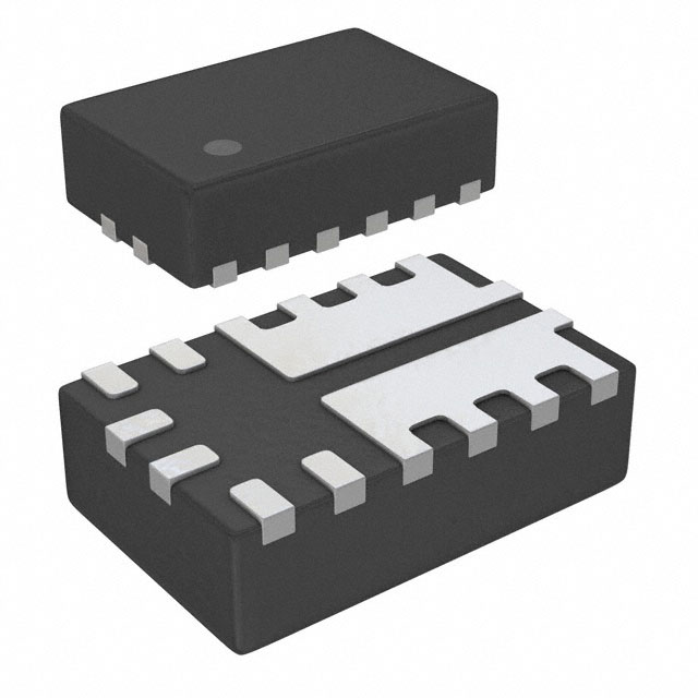
applications. The SLG59M1709V is packaged in a
space-efficient, low thermal resistance, RoHS-compliant
1.6 mm x 2.5 mm STQFN package
ON
1
NC
2
VIN
3
VIN
4
VIN
5
VIN
6
16
15
SLG59M1709V
VDD
GND
7
VIN
14
CAP
13
NC
8
12
VOUT
11
VOUT
10
VOUT
9
VOUT
VOUT
Features
•
•
•
•
•
•
Low Typical RDSON nFET: 4 mΩ
Maximum Continuous Switch Current: Up to 4 A
Supply Voltage: 2.5 V ≤ VDD ≤ 5.5 V
Wide Input Voltage Range: 0.8 V ≤ VIN ≤ VDD
Capacitor-adjustable Start-up and Inrush Current Control
Two-stage Overcurrent Protection:
• Fixed threshold, 8 A Active Current Limit
• Fixed 0.5 A Short-circuit Current Limit
• Operating Temperature: -40 °C to 85 °C
• Low θJA, 16-pin 1.6 mm x 2.5 mm STQFN Packaging
• Pb-Free / Halogen-Free / RoHS compliant
16-pin FC-STQFN
(Top View)
Applications
• Notebook Power Rail Switching
• Tablet Power Rail Switching
• Smartphone Power Rail Switching
Block Diagram
4 A @ 4 mΩ
VOUT
VIN
CIN
CLOAD
+2.5 to 5.5 V
VDD
Charge
Pump
Linear Ramp
Control
CAP
CSLEW
4 nF
Over Current and
Over Temperature
Protection
SW Closed
ON
CMOS Input
SW Open
GND
Datasheet
CFR0011-120-01
Revision 1.02
Page 1 of 20
4-Feb-2022
©2022 Renesas Electronics Corporation
�����
SLG59M1709V
An Ultra-small, 4 mΩ, 4 A Load Switch
with Multiple Protection Features
Pin Description
Pin #
Pin Name
Type
Pin Description
1
VDD
Power
With an internal 1.9 V VDD(UVLO) threshold, VDD supplies the power for the operation of
the load switch and internal control circuitry where its range is 2.5 V ≤ VDD ≤ 5.5 V. Bypass
the VDD pin to GND with a 0.1 μF (or larger) capacitor
2
NC
NC
3-7
VIN
MOSFET
Drain terminal of Power MOSFET (Pins 3-7 fused together). Connect a 10 µF (or larger)
low ESR capacitor from this pin to GND. Capacitors used at VIN should be rated at 10 V
or higher.
8-12
VOUT
MOSFET
Source terminal of Power MOSFET (Pins 8-12 fused together). Connect a low ESR
capacitor (up to 500 μF) from this pin to GND. Capacitors used at VOUT should be rated
at 10 V or higher.
13
NC
NC
14
CAP
Input
A low-ESR, stable dielectric, ceramic surface-mount capacitor connected from CAP pin to
GND sets the VOUT slew rate and overall turn-on time of the SLG59M1709V. For best
performance, the range for CSLEW values are 2 nF ≤ CSLEW ≤ 22 nF. Capacitors used at
the CAP pin should be rated at 10 V or higher.
15
GND
GND
Ground
16
ON
Input
A low-to-high transition on this pin closes the load switch. ON is an asserted-HIGH,
level-sensitive CMOS input with ON_VIL < 0.3 V and ON_VIH > 0.85 V. While there is an
internal pull down circuit to ground (~4 MΩ), connect this pin to the output of a
general-purpose output (GPO) from a microcontroller or other application processor.
No Connect
No Connect
Ordering Information
Part Number
Type
Production Flow
SLG59M1709V
STQFN 16L
Industrial, -40 °C to 85 °C
SLG59M1709VTR
STQFN 16L (Tape and Reel)
Industrial, -40 °C to 85 °C
Datasheet
CFR0011-120-01
Revision 1.02
Page 2 of 20
4-Feb-2022
©2022 Renesas Electronics Corporation
�����
SLG59M1709V
An Ultra-small, 4 mΩ, 4 A Load Switch
with Multiple Protection Features
Absolute Maximum Ratings
Parameter
VDD
VIN to GND
Description
Conditions
Min.
Typ.
Max.
Unit
--
--
6
V
-0.3
--
6
V
-0.3
--
VIN
V
ON and CAP Pin Voltages to GND
-0.3
--
6
V
Storage Temperature
-65
--
150
°C
--
V
--
V
Power Supply Pin to GND
Load Switch Input Voltage to GND
Load Switch Output Voltage to
VOUT to GND
GND
ON, CAP to
GND
TS
ESDHBM
ESDCDM
MSL
θJA
WDIS
MOSFET
IDSCONT
ESD Protection
Human Body Model
2000
--
ESD Protection
Charged Device Model
500
--
Moisture Sensitivity Level
Package Thermal Resistance,
Junction-to-Ambient
1
1.6 x 2.5 mm 16L STQFN; Determined using 1 in2, 1.2 oz. copper pads under each
VIN and VOUT on FR4 pcb material
--
35
--
°C/W
Package Power Dissipation
--
--
1.2
W
Continuous Current from VIN to
VOUT
--
--
4
A
--
--
6
A
MOSFET IDSPK Peak Current from VIN to VOUT
Maximum pulsed switch current, pulse
width < 1 ms, 1% duty cycle
Note: Stresses greater than those listed under “Absolute Maximum Ratings” may cause permanent damage to the device. This is a stress rating
only and functional operation of the device at these or any other conditions above those indicated in the operational sections of this
specification is not implied. Exposure to absolute maximum rating conditions for extended periods may affect reliability.
Electrical Characteristics
TA =-40 °C to 85 °C, unless otherwise noted.
Parameter
VDD
VDD(UVLO)
IDD
RDSON
Description
Conditions
Power Supply Voltage
Min.
Typ.
Max.
Unit
2.5
3.3
5.5
V
V
VDD Undervoltage Lockout
Threshold
VDD ↑
1.6
1.9
2.2
VDD ↓
1.5
1.8
2.2
V
Power Supply Current, when OFF
VDD = VIN = 5.5 V; ON = 0
--
1
2
μA
Power Supply Current, when ON
VDD = VIN = ON = 5.5 V; No Load
--
120
170
μA
VDD = VIN = 5 V;
TA = 25°C, IDS = 0.1 A
--
4
5.5
mΩ
5
6.8
mΩ
ON Resistance
VDD = VIN = 5 V;
TA = 85°C, IDS = 0.1 A
MOSFET
IDS
Current from VIN to VOUT
Continuous
--
--
4
A
IFET_OFF
MOSFET OFF Leakage Current
VDD = VIN = 5.5 V;
VOUT = 0 V; ON = 0 V
--
--
2
μA
VIN
ILIMIT
TON_Delay
Datasheet
CFR0011-120-01
0.8
--
VDD
V
Active Current Limit, IACL
Drain Voltage
VOUT > 0.3 V
6
8
10
A
Short-circuit Current Limit, ISCL
VOUT < 0.3 V
--
0.5
--
A
ON Delay Time
50% ON to VOUT Ramp Start
VDD = VIN = 5 V; CSLEW = 4 nF;
RLOAD = 20 Ω, CLOAD = 10 μF
--
200
--
μs
Revision 1.02
Page 3 of 20
4-Feb-2022
©2022 Renesas Electronics Corporation
�����
SLG59M1709V
An Ultra-small, 4 mΩ, 4 A Load Switch
with Multiple Protection Features
Electrical Characteristics (continued)
TA =-40 °C to 85 °C, unless otherwise noted.
Parameter
VOUT(SR)
Description
Conditions
Min.
Max.
Unit
10% VOUT to 90% VOUT ↑
Set by External CSLEW1
V/ms
Example: CSLEW = 4 nF;
VDD = VIN = 5 V; RLOAD = 20 Ω,
CLOAD = 10 μF
VOUT Slew Rate
Example: CSLEW = 4 nF;
VDD = VIN = 5 V; RLOAD = 20 Ω,
CLOAD = 10 μF
Total Turn-on Time
2.9
3.5
Set by External CSLEW1
50% ON to 90% VOUT ↑
TTotal_ON
2.5
Typ.
V/ms
ms
1.4
1.7
2
ms
OFF Delay Time
50% ON to VOUT Fall Start;
VDD = VIN = 5 V;
RLOAD = 20 Ω, no CLOAD
--
8
15
μs
Output Load Capacitance
CLOAD connected from VOUT to GND
--
--
500
μF
0.85
--
VDD
V
-0.3
0
0.3
V
--
1.5
--
μA
Thermal shutoff turn-on temperature
--
125
--
°C
THERMOFF Thermal shutoff turn-off temperature
--
100
--
°C
TOFF_Delay
CLOAD
ON_VIH
High Input Voltage on ON pin
ON_VIL
Low Input Voltage on ON pin
ION(LKG)
ON Pin Leakage Current
THERMON
ON = ON_VIH or ON = GND
Notes:
1. Refer to typical Timing Parameter vs. CSLEW performance charts for additional information when available.
TON_Delay, VOUT(SR), and TTotal_ON Timing Details
ON
50% ON
50% ON
TOFF_Delay
90% VOUT
VOUT
90% VOUT
TON_Delay
10% VOUT
10% VOUT
VOUT(SR) (V/ms)
TFALL
TTotal_ON
Datasheet
CFR0011-120-01
Revision 1.02
Page 4 of 20
4-Feb-2022
©2022 Renesas Electronics Corporation
�����
SLG59M1709V
An Ultra-small, 4 mΩ, 4 A Load Switch
with Multiple Protection Features
Typical Performance Characteristics
RDSON vs. VDD and Temperature
RDSON vs. VIN and VDD
Datasheet
CFR0011-120-01
Revision 1.02
Page 5 of 20
4-Feb-2022
©2022 Renesas Electronics Corporation
�����
SLG59M1709V
An Ultra-small, 4 mΩ, 4 A Load Switch
with Multiple Protection Features
VOUT Slew Rate vs. Temperature, VDD, VIN, and CSLEW
TTotal_ON vs. CSLEW, VIN, VDD, and Temperature
Datasheet
CFR0011-120-01
Revision 1.02
Page 6 of 20
4-Feb-2022
©2022 Renesas Electronics Corporation
�����
SLG59M1709V
An Ultra-small, 4 mΩ, 4 A Load Switch
with Multiple Protection Features
Timing Diagram - Basic Operation including Active Current Limit Protection
HIGH
VDD
1.9 V
LOW
Time
VIN
ON
TTotal_ON
TRISE
HIGH
VOUT
90%
TON_Delay
10%
Abnormal Step Load
Current Event
IACL
IACL
Active Current Limit
Operation
IDS
ISCL
ISCL
Nominal Steady State
Operation Resumes
ACL Threshold Triggered
Datasheet
CFR0011-120-01
Revision 1.02
Page 7 of 20
4-Feb-2022
©2022 Renesas Electronics Corporation
�����
SLG59M1709V
An Ultra-small, 4 mΩ, 4 A Load Switch
with Multiple Protection Features
Timing Diagram - Active Current Limit & Thermal Protection Operation
HIGH
VDD
1.9 V
LOW
Time
VIN
Nominal Steady State
Operation Resumes
ON
TTotal_ON
TRISE
VOUT
Active Current Limit
Operation
Thermal Protection
Operation
90%
TON_Delay
10%
IACL
Abnormal Step Load
Current Event
IACL
IDS
ISCL
ISCL
Die temp > THERMON
Datasheet
CFR0011-120-01
Revision 1.02
Page 8 of 20
Die temp < THERMOFF
4-Feb-2022
©2022 Renesas Electronics Corporation
�����
SLG59M1709V
An Ultra-small, 4 mΩ, 4 A Load Switch
with Multiple Protection Features
SLG59M1709V Power-Up/Power-Down Sequence Considerations
To ensure glitch-free power-up under all conditions, apply VDD first, followed by VIN after VDD exceeds 1.9 V. Then allow VIN to
reach 90% of its max value before toggling the ON pin from Low-to-High. Likewise, power-down in reverse order.
If VDD and VIN need to be powered up simultaneously, glitching can be minimized by having a suitable load capacitor. A 10 μF
CLOAD will prevent glitches for rise times of VDD and VIN higher than 2 ms.
If the ON pin is toggled HIGH before VDD and VIN have reached their steady-state values, the load switch timing parameters may
differ from datasheet specifications.
The slew rate of output VOUT follows a linear ramp set by a capacitor connected to the CAP pin. A larger capacitor value at the
CAP pin produces a slower ramp, reducing inrush current from capacitive loads.
SLG59M1709V Current Limiting Operation
The SLG59M1709V has two types of current limiting triggered by the output VOUT voltage.
1. Standard Current Limiting Mode (with Thermal Shutdown Protection)
When the VOUT voltage > 300 mV, the output current is initially limited to the Active Current Limit (IACL) specification listed in the
Electrical Characteristics table. The ACL monitor’s response time is very fast and is triggered within a few microseconds to sudden
(transient) changes in load current. When a load current overload is detected, the ACL monitor increases the FET resistance to
keep the current from exceeding the load switch’s IACL threshold. During active current-limit operation, VOUT is also reduced by
IACL x RDSON(ACL). This observed behavior is illustrated in the timing diagrams on Pages 7 and 8.
However, if a load-current overload condition persists where the die temperature rises because of the increased FET resistance,
the load switch’s internal Thermal Shutdown Protection circuit can be activated. If the die temperature exceeds the listed
THERMON specification, the FET is shut OFF completely, thereby allowing the die to cool. When the die cools to the listed
THERMOFF temperature threshold, the FET is allowed to turn back on. This process may repeat as long as the output current
overload condition persists.
2. Short Circuit Current Limiting Mode (with Thermal Shutdown Protection)
When the VOUT voltage < 300 mV (which is the case with a hard short, such as a solder bridge on the power rail), the load switch’s
internal Short-circuit Current Limit (SCL) monitor limits the FET current to approximately 500 mA (the ISCL threshold). While the
internal Thermal Shutdown Protection circuit remains enabled and since the ISCL threshold is much lower than the IACL threshold,
thermal shutdown protection may become activated only at higher ambient temperatures.
SLG59M1709V Start-up Inrush Current Considerations with Capacitive Loads
In distributed power applications, the SLG59M1709V is generally implemented on the outboard or downstream side of switching
regulator dc/dc converters with internal overcurrent protection. As an adjustable output voltage slew-rate load switch, it is important to understand the start-up operation of the SLG59M1709V with capacitive loads. An equivalent circuit of the SLG59M1709V’s
slew-rate control loop with capacitors at its VIN and VOUT pins is shown in Figure 1:
Datasheet
CFR0011-120-01
Revision 1.02
Page 9 of 20
4-Feb-2022
©2022 Renesas Electronics Corporation
�����
SLG59M1709V
An Ultra-small, 4 mΩ, 4 A Load Switch
with Multiple Protection Features
SLG59M1709V Start-up Inrush Current Considerations with Capacitive Loads (continued)
CSLEW
Figure 1. SLG59M1709V’s Equivalent Slew-rate Control Loop Circuit.
For a desired VOUT slew-rate (VOUT(SR)), a corresponding CSLEW value is selected. At the VOUT pin and with ON = LOW, the
internal FET is OFF, VOUT is initially at 0V, and there is no stored charge on CLOAD. When a low-to-high transition is applied to
the IC’s ON pin, an internal current source (I1) is enabled which, in turn, charges the external slew-rate capacitor, CSLEW. The
SLG59M1709V’s internal micropower op amp sets the circuit’s VOUT(SR) based on the slew rate of the nodal voltage at its
non-inverting pin (the voltage at the CAP pin).
As a function of VOUT(SR) and CLOAD, a 1st-order expression for the circuit’s FET current (and inrush current) when a low-to-high
transition on the ON pin is applied becomes:
Start-up Current IDS or IINRUSH = VOUT(SR) x CLOAD
From the expression above and for a given VOUT(SR), CLOAD determines the magnitude of the inrush current; that is, for large
values of CLOAD, large inrush currents can result. If the inrush currents are large enough to trigger the overcurrent protection of
an upstream dc/dc converter, the system can be shut down.
In applications where the desired VOUT(SR) is fast and CLOAD is very large (>200 µF), there is a secondary effect on the observed
VOUT(SR) attributed to the SLG59M1709V’s internal short-circuit current limit monitor (its SCL monitor). If the resultant inrush
current is larger than the IC’s ISCL threshold, the SCL current monitor limits the inrush current and the current to charge CLOAD
until the ISCL OFF threshold is crossed (~0.3V). During the time the SCL monitor’s been activated, the inrush current profile may
exhibit an observable reduction in VOUT(SR) as shown in Figure 2 where CSLEW was set to 4nF and 470 µF was chosen for CLOAD.
Datasheet
CFR0011-120-01
Revision 1.02
Page 10 of 20
4-Feb-2022
©2022 Renesas Electronics Corporation
�����
SLG59M1709V
An Ultra-small, 4 mΩ, 4 A Load Switch
with Multiple Protection Features
SLG59M1709V Start-up Inrush Current Considerations with Capacitive Loads (continued)
Figure 2. A SLG59M1709V with CSLEW set to 4nF and 470µF for CLOAD. CLOAD-to-CSLEW
ratio is greater than 33,600. Note that the internal SCL monitor’s been triggered and VOUT(SR) is reduced until VOUT reaches ~0.3V.
A closer analysis of the IC’s internal slew-control large-scale yields the following:
ISCL
I1
= MSR x
CLOAD
CSLEW
where
ISCL = IC’s short-circuit current limit threshold, typically 0.5A;
MSR = An internal slew-rate multiplier from the IC’s CAP pin to the VOUT pin;
I1 = An internal current source to charge the external capacitor (CSLEW).
Rearranging the equation to isolate both CLOAD and CSLEW yields the following:
CLOAD
ISCL
= I xM
CSLEW
1
SR
For the SLG59M1709V device, the right-hand side of the expression is approximately 33,600 after taking into account part-to-part
variations because of process, voltage, and temperature.
Referring to the configuration of Figure 2’s scope capture, the CLOAD-to-CSLEW ratio is 117,500 (470µF/4nF) where it is evident
that the SCL monitor circuit is charging CLOAD shortly after a low-to-high ON transition. If it is desired to avoid a reduction in
VOUT(SR), the choices are decreasing CLOAD and/or increasing CSLEW so that the ratio is always less than 33,600 including taking
into account external capacitor tolerances for initial accuracy and temperature.
As shown in Figure 3, it was chosen to reduce VOUT(SR) by increasing CSLEW to 15nF while keeping CLOAD at 470µF. With this
configuration, the ratio of CLOAD to CSLEW is about 31,333 (smaller than 33,600). Upon a low-to-high transition on the ON pin,
the VOUT increases smoothly with no evidence of SCL monitor’s interaction.
Datasheet
CFR0011-120-01
Revision 1.02
Page 11 of 20
4-Feb-2022
©2022 Renesas Electronics Corporation
�����
SLG59M1709V
An Ultra-small, 4 mΩ, 4 A Load Switch
with Multiple Protection Features
SLG59M1709V Start-up Inrush Current Considerations with Capacitive Loads (continued)
Figure 3. A SLG59M1709V with CSLEW set to 15nF and 470µF retained for CLOAD.
CLOAD-to-CSLEW ratio is smaller than 33,600. Note smooth VOUT transition.
Power Dissipation
The junction temperature of the SLG59M1709V depends on different factors such as board layout, ambient temperature, and
other environmental factors. The primary contributor to the increase in the junction temperature of the SLG59M1709V is the power
dissipation of its power MOSFET. Its power dissipation and the junction temperature in nominal operating mode can be calculated
using the following equations:
PD = RDSON x IDS2
where:
PD = Power dissipation, in Watts (W)
RDSON = Power MOSFET ON resistance, in Ohms (Ω)
IDS = Output current, in Amps (A)
and
TJ = PD x θJA + TA
where:
TJ = Junction temperature, in Celsius degrees (°C)
θJA = Package thermal resistance, in Celsius degrees per Watt (°C/W)
TA = Ambient temperature, in Celsius degrees (°C)
Datasheet
CFR0011-120-01
Revision 1.02
Page 12 of 20
4-Feb-2022
©2022 Renesas Electronics Corporation
�����
SLG59M1709V
An Ultra-small, 4 mΩ, 4 A Load Switch
with Multiple Protection Features
Power Dissipation (continued)
During active current-limit operation, the SLG59M1709V’s power dissipation can be calculated by taking into account the voltage
drop across the load switch (VIN-VOUT) and the magnitude of the output current in active current-limit operation (IACL):
PD = (VIN-VOUT) x IACL or
PD = (VIN – (RLOAD x IACL)) x IACL
where:
PD = Power dissipation, in Watts (W)
VIN = Input Voltage, in Volts (V)
RLOAD = Load Resistance, in Ohms (Ω)
IACL = Output limited current, in Amps (A)
VOUT = RLOAD x IACL
For more information on GreenFET load switch features, please visit our website and see App Note “AN-1068 GreenFET and
High Voltage GreenFET Load Switch Basics”.
Datasheet
CFR0011-120-01
Revision 1.02
Page 13 of 20
4-Feb-2022
©2022 Renesas Electronics Corporation
�����
SLG59M1709V
An Ultra-small, 4 mΩ, 4 A Load Switch
with Multiple Protection Features
Layout Guidelines:
1. The VDD pin needs a 0.1 µF (or larger) external capacitor to smooth pulses from the power supply. Locate this capacitor as
close as possible to the SLG59M1709V’s pin 1.
2. Since the VIN and VOUT pins dissipate most of the heat generated during high-load current operation, it is highly recommended
to make power traces as short, direct, and wide as possible. A good practice is to make power traces with an absolute minimum
widths of 15 mils (0.381 mm) per Ampere. A representative layout, shown in Figure 4, illustrates proper techniques for heat to
transfer as efficiently as possible out of the device;
3. To minimize the effects of parasitic trace inductance on normal operation, it is recommended to connect input CIN and output
CLOAD low-ESR capacitors as close as possible to the SLG59M1709V's VIN and VOUT pins;
4. The GND pin should be connected to system analog or power ground plane.
SLG59M1709V Evaluation Board:
А GreenFET Evaluation Board for SLG59M1709V is designed according to the statements above and is illustrated on Figure 4.
Please note that evaluation board has D_Sense and S_Sense pads. They cannot carry high currents and dedicated only for
RDSON evaluation.
Figure 4. SLG59M1709V Evaluation Board.
Datasheet
CFR0011-120-01
Revision 1.02
Page 14 of 20
4-Feb-2022
©2022 Renesas Electronics Corporation
�����
SLG59M1709V
GND
GND
1
IOUT
1
GND
1
ON
1
C4
3 .9 nF
U1
1
2
3
4
5
6
7
VDD
NC
VIN
VIN
VIN
VIN
VIN
ON
GND
CAP
NC
VOUT
VOUT
VOUT
VOUT
VOUT
1
3
5
7
9
2
4
6
8
10
1
C2
10u
1
1
2
3
4
1
2
3
4
SOURCE
1
2
3
4
DRAIN
GND
D/VIN
GND
S_SENSE
1
2
3
4
1
C1
22u
D_SENSE
CAP/RSET Array
16
15
14
13
12
11
10
9
8
1
VDD
1
2
3
VDD
1
1
FAULT#
1
An Ultra-small, 4 mΩ, 4 A Load Switch
with Multiple Protection Features
S/VOUT
Figure 5. SLG59M1709V Evaluation Board Connection Circuit.
Basic Test Setup and Connections
Figure 6. Typical connections for GreenFET Evaluation.
EVB Configuration
1. Connect oscilloscope probes to VIN, VOUT, ON, etc.;
2. Turn on Power Supply 1 and set desired VDD from 2.5 V…5.5 V range;
3. Turn on Power Supply 2 and set desired VIN from 0.8 V…VDD range;
4. Toggle the ON signal High or Low to observe SLG59M1709V operation.
Datasheet
CFR0011-120-01
Revision 1.02
Page 15 of 20
4-Feb-2022
©2022 Renesas Electronics Corporation
�����
SLG59M1709V
An Ultra-small, 4 mΩ, 4 A Load Switch
with Multiple Protection Features
Package Top Marking System Definition
Pin 1 Identifier
PPPPP
WWNNN
ARR
Part Code
Date Code + LOT Code
Assembly + Rev. Code
PPPPP - Part ID Field
WW - Date Code Field1
NNN - Lot Traceability Code Field1
A - Assembly Site Code Field 2
RR - Part Revision Code Field2
Note 1: Each character in code field can be alphanumeric A-Z and 0-9
Note 2: Character in code field can be alphabetic A-Z
Datasheet
CFR0011-120-01
Revision 1.02
Page 16 of 20
4-Feb-2022
©2022 Renesas Electronics Corporation
�����
SLG59M1709V
An Ultra-small, 4 mΩ, 4 A Load Switch
with Multiple Protection Features
Package Drawing and Dimensions
16 Lead STQFN Package 1.6 mm x 2.5 mm (Fused Lead)
Datasheet
CFR0011-120-01
Revision 1.02
Page 17 of 20
4-Feb-2022
©2022 Renesas Electronics Corporation
�����
SLG59M1709V
An Ultra-small, 4 mΩ, 4 A Load Switch
with Multiple Protection Features
SLG59M1709V 16-pin STQFN PCB Landing Pattern
Datasheet
CFR0011-120-01
Revision 1.02
Page 18 of 20
4-Feb-2022
©2022 Renesas Electronics Corporation
�����
SLG59M1709V
An Ultra-small, 4 mΩ, 4 A Load Switch
with Multiple Protection Features
Tape and Reel Specifications
Max Units
Leader (min)
Nominal
Reel &
Package # of
Package Size
Hub Size
Length
Type
Pins
per Reel per Box
Pockets
[mm]
[mm]
[mm]
STQFN
16L
1.6x2.5mm
0.4P FCA
Green
1.6x2.5x
0.55mm
16
3000
3000
178/60
100
400
Trailer (min)
Pockets
Length
[mm]
Tape
Width
[mm]
100
400
8
Part
Pitch
[mm]
4
Carrier Tape Drawing and Dimensions
Package
Type
Pocket BTM Pocket BTM
Length
Width
STQFN 16L
1.6x2.5mm
0.4P FCA
Green
Pocket
Depth
Index Hole
Pitch
Pocket
Pitch
Index Hole
Diameter
Index Hole Index Hole
to Tape
to Pocket Tape Width
Edge
Center
A0
B0
K0
P0
P1
D0
E
F
W
1.8
2.8
0.7
4
4
1.55
1.75
3.5
8
P0
D0
E
Y
W
F
Section Y-Y
B0
CL
K0
Y
P1
A0
Refer to EIA-481 specification
Recommended Reflow Soldering Profile
Please see IPC/JEDEC J-STD-020: latest revision for reflow profile based on package volume of 2.2 mm3 (nominal). More
information can be found at www.jedec.org.
Datasheet
CFR0011-120-01
Revision 1.02
Page 19 of 20
4-Feb-2022
©2022 Renesas Electronics Corporation
�����
SLG59M1709V
An Ultra-small, 4 mΩ, 4 A Load Switch
with Multiple Protection Features
Revision History
Date
Version
2/4/2022
1.02
Updated Company name and logo
Fixed typos
10/19/2018
1.01
Updated style and formatting
Added Layout Guidelines
Fixed typos
1/30/2017
1.00
Production Release
Datasheet
CFR0011-120-01
Change
Revision 1.02
Page 20 of 20
4-Feb-2022
©2022 Renesas Electronics Corporation
�IMPORTANT NOTICE AND DISCLAIMER
RENESAS ELECTRONICS CORPORATION AND ITS SUBSIDIARIES (“RENESAS”) PROVIDES TECHNICAL
SPECIFICATIONS AND RELIABILITY DATA (INCLUDING DATASHEETS), DESIGN RESOURCES (INCLUDING
REFERENCE DESIGNS), APPLICATION OR OTHER DESIGN ADVICE, WEB TOOLS, SAFETY INFORMATION, AND
OTHER RESOURCES “AS IS” AND WITH ALL FAULTS, AND DISCLAIMS ALL WARRANTIES, EXPRESS OR IMPLIED,
INCLUDING, WITHOUT LIMITATION, ANY IMPLIED WARRANTIES OF MERCHANTABILITY, FITNESS FOR A
PARTICULAR PURPOSE, OR NON-INFRINGEMENT OF THIRD PARTY INTELLECTUAL PROPERTY RIGHTS.
These resources are intended for developers skilled in the art designing with Renesas products. You are solely responsible
for (1) selecting the appropriate products for your application, (2) designing, validating, and testing your application, and (3)
ensuring your application meets applicable standards, and any other safety, security, or other requirements. These
resources are subject to change without notice. Renesas grants you permission to use these resources only for
development of an application that uses Renesas products. Other reproduction or use of these resources is strictly
prohibited. No license is granted to any other Renesas intellectual property or to any third party intellectual property.
Renesas disclaims responsibility for, and you will fully indemnify Renesas and its representatives against, any claims,
damages, costs, losses, or liabilities arising out of your use of these resources. Renesas' products are provided only subject
to Renesas' Terms and Conditions of Sale or other applicable terms agreed to in writing. No use of any Renesas resources
expands or otherwise alters any applicable warranties or warranty disclaimers for these products.
(Rev.1.0 Mar 2020)
Corporate Headquarters
Contact Information
TOYOSU FORESIA, 3-2-24 Toyosu,
Koto-ku, Tokyo 135-0061, Japan
www.renesas.com
For further information on a product, technology, the most
up-to-date version of a document, or your nearest sales
office, please visit:
www.renesas.com/contact/
Trademarks
Renesas and the Renesas logo are trademarks of Renesas
Electronics Corporation. All trademarks and registered
trademarks are the property of their respective owners.
© 2021 Renesas Electronics Corporation. All rights reserved.
�