SLG59M1568V
7.3 mΩ, 9 A GreenFET
Load Switch with Discharge
����
General Description
Pin Configuration
The SLG59M1568V is designed for load switching application.
The part comes with one 9 A rated MOSFET switched on by
an ON control pin. MOSFET turn on time is independently
adjusted by an external capacitor.
MOS_D
1
14
MOS_D
2
13
MOS_S
MOS_S
ON_MOS
3
12
CAP
4
11
GND
ON_MOS
5
10
CAP
MOS_D
6
9
MOS_D
7
8
MOS_S
MOS_S
Features
•
•
•
•
•
•
•
•
VDD
One 9 A independent MOSFET
Integrated VGS Charge Pump
Internal discharge for gate and source
User selectable ramp control by external capacitor
Protected by thermal shutdown with current limit
Pb-Free / RoHS Compliant
Halogen-Free
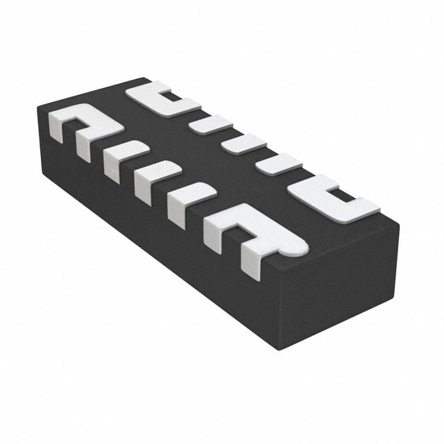
STDFN 14L, 1 x 3 x 0.55 mm
14-pin STDFN
(Top View)
Target Applications
• Consumer Electronics
• Portable: Tablets, Notebooks
• PCs and PC peripherals
• Commercial and Industrial Electronics
• Printers
• Servers
• Embedded PCs
• Data Communications Equipment
Block Diagram
9 A @ 7.3 mΩ
MOS_D
+2.5 to 5.5 V
CAP
MOS_S
Charge
Pump
PIN10
Linear Ramp
Control
PIN12
Over Current and
Over Temperature
Protection
PIN3
ON/OFF
CMOS Input
PIN5
©2022 Renesas Electronics Corporation
000-0059M1568-106
Rev 1.06
Revised February 7, 2022
�SLG59M1568V
����
Pin Description
Pin #
Pin Name
Type
Pin Description
1
MOS_D
MOSFET
Drain of MOSFET
2
MOS_D
MOSFET
3
ON_MOS
Input
4
VDD
Power
5
ON_MOS
Input
6
MOS_D
MOSFET
Drain of MOSFET
7
MOS_D
MOSFET
Drain of MOSFET
8
MOS_S
MOSFET
Source of MOSFET
9
MOS_S
MOSFET
Source of MOSFET
10
CAP
Input
Sets ramp and turn on time for MOSFET. Tied to Pin 12 on PCB.
11
GND
GND
Ground
12
CAP
Input
Sets ramp and turn on time for MOSFET. Tied to Pin 10 on PCB.
13
MOS_S
MOSFET
Source of MOSFET
14
MOS_S
MOSFET
Source of MOSFET
Drain of MOSFET
Turns on MOS (4 MΩ pull down resistor). Tied to Pin 5 on PCB.
VDD Power for Load Switch Control
Turns on MOS (4 MΩ pull down resistor). Tied to Pin 3 on PCB.
Ordering Information
Part Number
Type
Production Flow
SLG59M1568V
STDFN 14L
Industrial, -40 °C to 85 °C
SLG59M1568VTR
STDFN 14L (Tape and Reel)
Industrial, -40 °C to 85 °C
000-0059M1568-106
Page 2 of 10
�SLG59M1568V
����
Absolute Maximum Ratings
Parameter
VDD
TS
ESDHBM
WDIS
IDSMAX
Description
Conditions
Power Supply
Storage Temperature
ESD Protection
Human Body Model
Min.
Typ.
Max.
Unit
--
--
6
V
-65
--
150
°C
2000
--
--
V
--
--
1.2
W
9
A
12
A
Package Power Dissipation
Max Operating Current
MOSFET IDSPK Peak Current from Drain to Source
For no more than 10 continuous seconds
out of every 100 seconds
--
--
Note: Stresses greater than those listed under “Absolute Maximum Ratings” may cause permanent damage to the device. This is a stress rating
only and functional operation of the device at these or any other conditions above those indicated in the operational sections of this
specification is not implied. Exposure to absolute maximum rating conditions for extended periods may affect reliability.
Electrical Characteristics
TA = -40 °C to 85 °C (unless otherwise stated)
Parameter
VDD
IDD
RDSON
Description
Conditions
Power Supply Voltage
Power Supply Current when OFF
Typ.
Max.
2.5
--
5.5
V
--
0.1
1
µA
--
50
75
µA
--
7.3
9
mΩ
TA = 70°C; IDS = 100 mA
--
8
11
mΩ
8.5
11.5
mΩ
--
9
A
1.0
5.0
VDD
V
--
300
500
µs
TA = 85°C; IDS = 100 mA
MOSFET
IDS
VMOS_D
TON_Delay
Current from Drain to Source
Continuous
Drain Voltage
ON Delay Time
50% ON to Ramp Begin
--
Configurable 1
50% ON to 90% VS
TTotal_ON
Total Turn On Time
Example: CAP (Pin 10 & 12) share
a single 4nF capacitor,
VDD = VD = 5 V, CLOAD = 10 µF,
RLOAD = 20 Ω
--
Slew Rate
CLOAD
Output Load Capacitance
1.1
ms
--
ms
Configurable 1
10% VS to 90% VS
VS(SR)
Unit
TA = 25°C; IDS = 100 mA
Power Supply Current when ON
ON Resistance
Min.
V/ms
Example: CAP (Pin 10 & 12) share
a single 4nF capacitor,
VDD = VD = 5 V, CLOAD = 10 µF,
RLOAD = 20 Ω
--
6.0
--
V/ms
CLOAD connected from MOS_S to
GND
--
--
1000
µF
Discharge Resistance
100
210
300
Ω
ON_VIH
High Input Voltage on ON pin
0.85
--
VDD
V
ON_VIL
Low Input Voltage on ON pin
RDIS
-0.3
0
0.3
V
Active Current Limit
MOSFET will automatically limit current when VS > 250 mV
--
12.0
--
A
Short Circuit Current Limit
MOSFET will automatically limit current when VS < 250 mV
--
0.5
--
A
Thermal shutoff turn-on temperature
--
125
--
°C
THERMOFF Thermal shutoff turn-off temperature
--
100
--
°C
THERMTIME Thermal shutoff time
--
--
1
ms
ILIMIT
THERMON
000-0059M1568-106
Page 3 of 10
�SLG59M1568V
����
TA = -40 °C to 85 °C (unless otherwise stated)
Parameter
Description
Conditions
TOFF_Delay
OFF Delay Time
50% ON to VS Fall, VDD = VD = 5 V
Min.
Typ.
Max.
Unit
--
--
15
µs
Notes:
1. Refer to table for configuration details.
TTotal_ON, TON_Delay and Slew Rate Measurement
ON
50% ON
50% ON
TOFF_Delay
90% VS
VS
90% VS
TON_Delay
10% VS
10% VS
VS(SR) (V/ms)
TFALL
TTotal_ON
000-0059M1568-106
Page 4 of 10
�SLG59M1568V
����
Slew Rate vs. CAP, VMOS_D, and VDD
TTotal_ON vs. CAP, VMOS_D, and VDD
000-0059M1568-106
Page 5 of 10
�SLG59M1568V
����
Package Top Marking System Definition
Part Code
Pin 1 Identifier
PPDDL
Lot #
Date Code
000-0059M1568-106
Page 6 of 10
�SLG59M1568V
����
Package Drawing and Dimensions
14 Lead STDFN Package 1 mm x 3 mm (Fused Lead)
000-0059M1568-106
Page 7 of 10
�SLG59M1568V
����
Tape and Reel Specifications
Package
Type
# of
Pins
Nominal
Package
Size
STDFN
14L
1x3mm
0.4P FC
14
1x3x0.55mm
Trailer A
Leader B
Pocket Tape (mm)
Max
Reel &
Units per Units Hub Size
Reel
Pockets Length Pockets Length Width
Pitch
per Box
(mm)
(mm)
(mm)
3000
3000
178/60
100
400
100
400
8
4
Carrier Tape Drawing and Dimensions
Pocket BTM Pocket BTM
Length
Width
Package
[mm]
[mm]
Type
STDFN 14L
1x3mm 0.4P
FC
Pocket
Depth
[mm]
Index Hole
Pitch
[mm]
Pocket
Pitch
[mm]
Index Hole
Diameter
[mm]
Index Hole Index Hole
to Tape
to Pocket Tape Width
Edge
Center
[mm]
[mm]
[mm]
A0
B0
K0
P0
P1
D0
E
F
W
1.15
3.15
0.7
4
4
1.5
1.75
3.5
8
Recommended Reflow Soldering Profile
Please see IPC/JEDEC J-STD-020: latest revision for reflow profile based on package volume of 1.65 mm3 (nominal). More
information can be found at www.jedec.org.
000-0059M1568-106
Page 8 of 10
�SLG59M1568V
����
Recommended Land Pattern and PCB Layout
000-0059M1568-106
Page 9 of 10
�SLG59M1568V
����
Revision History
Date
Version
2/7/2022
1.06
Renesas rebranding
Fixed typos
4/13/2018
1.05
Fixed typo in Block Diagram
Fixed typo in Abs Max Table
Clean up EC Table Parameters and Conditions
Updated Charts
3/15/2016
1.04
Fixed RDSon values
000-0059M1568-106
Change
Page 10 of 10
�IMPORTANT NOTICE AND DISCLAIMER
RENESAS ELECTRONICS CORPORATION AND ITS SUBSIDIARIES (“RENESAS”) PROVIDES TECHNICAL
SPECIFICATIONS AND RELIABILITY DATA (INCLUDING DATASHEETS), DESIGN RESOURCES (INCLUDING
REFERENCE DESIGNS), APPLICATION OR OTHER DESIGN ADVICE, WEB TOOLS, SAFETY INFORMATION, AND
OTHER RESOURCES “AS IS” AND WITH ALL FAULTS, AND DISCLAIMS ALL WARRANTIES, EXPRESS OR IMPLIED,
INCLUDING, WITHOUT LIMITATION, ANY IMPLIED WARRANTIES OF MERCHANTABILITY, FITNESS FOR A
PARTICULAR PURPOSE, OR NON-INFRINGEMENT OF THIRD PARTY INTELLECTUAL PROPERTY RIGHTS.
These resources are intended for developers skilled in the art designing with Renesas products. You are solely responsible
for (1) selecting the appropriate products for your application, (2) designing, validating, and testing your application, and (3)
ensuring your application meets applicable standards, and any other safety, security, or other requirements. These
resources are subject to change without notice. Renesas grants you permission to use these resources only for
development of an application that uses Renesas products. Other reproduction or use of these resources is strictly
prohibited. No license is granted to any other Renesas intellectual property or to any third party intellectual property.
Renesas disclaims responsibility for, and you will fully indemnify Renesas and its representatives against, any claims,
damages, costs, losses, or liabilities arising out of your use of these resources. Renesas' products are provided only subject
to Renesas' Terms and Conditions of Sale or other applicable terms agreed to in writing. No use of any Renesas resources
expands or otherwise alters any applicable warranties or warranty disclaimers for these products.
(Rev.1.0 Mar 2020)
Corporate Headquarters
Contact Information
TOYOSU FORESIA, 3-2-24 Toyosu,
Koto-ku, Tokyo 135-0061, Japan
www.renesas.com
For further information on a product, technology, the most
up-to-date version of a document, or your nearest sales
office, please visit:
www.renesas.com/contact/
Trademarks
Renesas and the Renesas logo are trademarks of Renesas
Electronics Corporation. All trademarks and registered
trademarks are the property of their respective owners.
© 2021 Renesas Electronics Corporation. All rights reserved.
�