SLG7NT614V
Ultra-small 22 mΩ 4 A Load Switch
with Reverse Current Blocking
����
General Description
Pin Configuration
The SLG7NT614V is a 22 mΩ 4 A single-channel load switch
that is able to switch 1 to 5 V power rails. The product is
packaged in an ultra-small 1.5 x 2.0 mm package.
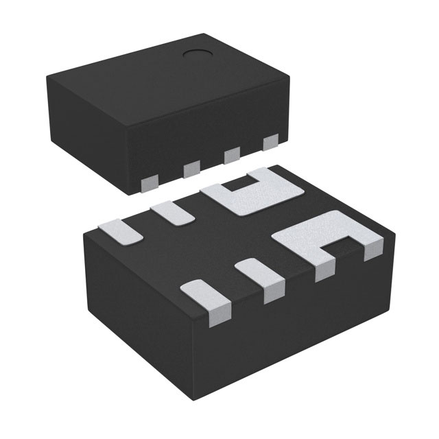
• 1.5 x 2.0 mm FC-TDFN 8L package (2 fused pins for drain
and 2 fused pins for source)
• Logic level ON pin capable of supporting 0.85 V CMOS
Logic
• User selectable ramp rate with external capacitor
• 22 mΩ RDSONwhile supporting 4 A
• Two Over Current Protection Modes
• Short Circuit Current Limit
• Active Current Limit
• Over Temperature Protection
• Pb-Free / Halogen-Free / RoHS compliant
• Operating Temperature: -40 °C to 85°C
• Operating Voltage: 2.5 V to 5.5 V
1
ON
2
VIN
3
VIN
4
SLG7NT614V
Features
VDD
8
GND
7
CAP
6
VOUT
5
VOUT
8-pin FC-TDFN
(Top View)
Applications
• Notebook Power Rail Switching
• Tablet Power Rail Switching
• Smartphone Power Rail Switching
Block Diagram
4 A @ 22 mΩ
Reverse
Blocking
VIN
+2.5 to 5.5 V
CAP
VOUT
Charge
Pump
Linear Ramp
Control
Over Current and
Over Temperature
Protection
ON
©2022 Renesas Electronics Corporation
000-007NT614-101
CMOS Input
Rev 1.01
Revised February 7, 2022
�SLG7NT614V
����
Pin Description
Pin #
Pin Name
Type
Pin Description
1
VDD
PWR
VDD power for load switch control (2.5 V to 5.5 V)
2
ON
Input
Turns MOSFET ON (4 MΩ pull down resistor)
CMOS input with VIL < 0.3 V, VIH > 0.85 V
3
VIN
MOSFET
Drain of Power MOSFET (fused with pin 4)
4
VIN
MOSFET
Drain of Power MOSFET (fused with pin 3)
5
VOUT
MOSFET
Source of Power MOSFET (fused with pin 6)
6
VOUT
MOSFET
Source of Power MOSFET (fused with pin 5)
7
CAP
Input
Capacitor for controlling power rail ramp rate
8
GND
GND
Ground
Ordering Information
Part Number
Type
Production Flow
SLG7NT614V
FC-TDFN 8L
Industrial, -40 °C to 85 °C
SLG7NT614VTR
FC-TDFN 8L (Tape and Reel)
Industrial, -40 °C to 85 °C
000-007NT614-101
Page 2 of 10
�SLG7NT614V
����
Absolute Maximum Ratings
Parameter
VDD
TS
ESDHBM
WDIS
Description
Conditions
Power Supply
Storage Temperature
ESD Protection
Human Body Model
Min.
Typ.
Max.
Unit
--
--
7
V
-65
--
150
°C
2000
--
--
V
--
--
1
W
--
--
6
A
Package Power Dissipation
MOSFET IDSPK Peak Current from Drain to Source For no more than 1 ms with 1% duty cycle
Note: Stresses greater than those listed under “Absolute Maximum Ratings” may cause permanent damage to the device. This is a stress rating
only and functional operation of the device at these or any other conditions above those indicated in the operational sections of this
specification is not implied. Exposure to absolute maximum rating conditions for extended periods may affect reliability.
Electrical Characteristics
TA = -40 °C to 85 °C (unless otherwise stated)
Parameter
Description
Conditions
VDD
Power Supply Voltage
-40 °C to 85 °C
IDD
Power Supply Current (PIN 1)
RDSON
Static Drain to Source
ON Resistance
IDS
Operating Current
VIN
Drain Voltage
TON_Delay
ON pin Delay Time
Min.
Typ.
Max.
Unit
2.5
--
5.5
V
when OFF
--
--
1
µA
when ON, No load
--
70
100
µA
TA 25°C @ 100 mA
--
22
28
mΩ
TA 70°C @ 100 mA
--
25
30
mΩ
TA 85°C @ 100 mA
--
27
31
mΩ
VIN = 1.0 V to 5.5 V
--
--
4
A
1.0
--
VDD
V
300
500
50% ON to Ramp Begin
0
Configurable 1
50% ON to 90% VOUT
TTotal_ON
Total Turn On Time
Example: CAP (PIN 7) = 4 nF, VDD
= VIN = 5 V, Source_Cap = 10 µF,
IDS = 100 mA
--
TSLEWRATE
IREVERSE
Slew Rate
Reverse Blocking Current
CAPSOURCE Source Cap
--
ms
Configurable 1
10% VOUT to 90% VOUT
Example: CAP (PIN 7) = 4 nF, VDD
= VIN = 5 V, Source_Cap = 10 µF,
IDS = 100 mA
1.96
--
3.0
µs
ms
V/ms
--
V/ms
VOUT = 5.0, VIN = 0 V
--
1
--
µA
Source to GND
--
--
500
µF
ON_VIH
High Input Voltage on ON pin
0.85
--
VDD
V
ON_VIL
Low Input Voltage on ON pin
-0.3
0
0.3
V
Active Current Limit
MOSFET will automatically limit current when VOUT > 250 mV
--
6.0
--
A
Short Circuit Current Limit
MOSFET will automatically limit current when VOUT < 250 mV
--
0.5
--
A
Thermal shutoff turn-on temperature
--
125
--
°C
THERMOFF Thermal shutoff turn-off temperature
--
100
--
°C
THERMTIME Thermal shutoff time
--
--
1
ms
--
7.5
15
µs
ILIMIT
THERMON
TOFF_Delay
OFF Delay Time
50% ON to VOUT Fall,
VDD = VIN = 5 V
Notes:
1. Refer to table for configuration details.
000-007NT614-101
Page 3 of 10
�����
SLG7NT614V
SLG7NT614V Turn ON
The normal power on sequence is first VDD, with VIN only being applied after VDD is > 1 V, and then ON after VIN is at least
90% of final value. The normal power off sequence is the power on sequence in reverse.
If VDD and VIN are turned on at the same time then it is possible that a voltage glitch will appear on VOUT before VDD achieves
1V which is the VT of the main MOSFET. The size of the glitch is dependent on source and drain capacitance loading and the
ramp rate of VDD & VIN.
SLG7NT614V Turn ON
The VOUT ramp follows a linear path, not an RC limitation provided the ramp is slow enough to not be current limited by load
capacitance.
SLG7NT614V Current Limiting
The SLG7NT614V has two forms of current limiting.
Standard Current Limiting Mode
Current is measured by mirroring the current through the main MOSFET. The mirrored current is then sent through a resistor
creating a voltage V(i) proportional to the MOSFET current. The V(i) is then compared with a Band Gap voltage V(BG). If V(i)
exceeds the Band Gap voltage then the voltage V(g) on the gate of the main MOSFET is reduced. The V(g) continues to drop
until V(i) < V(BG). This response is a closed loop response and is therefore very fast and current limits in less than a few
micro-seconds. There is no difference between peak or constant current limit.
Temperature Cutoff
However, as the V(g) drops the Rds(ON) of the main MOSFET will increase, thus limiting the current, but also increasing the
power dissipation of the IC. The IC is very small and cannot dissipate much power. Therefore, if a current limit condition is
sustained the IC will heat up. If the temperature exceeds approximately 120°C, then V(g) will be brought low completely shutting
off the main MOSFET. As the die cools the MOSFET will be turned back on at 100°C.
If the current limiting condition has not been mitigated then the die will again heat up to 120°C and the process will repeat.
Short Circuit Current Limiting Mode
When V(VOUT) < 250 mV, which is the case if there is a solder bridge during the manufacturing process or a hard short on the
power rail, then the current is limited to approximately 500 mA. This current limit is accomplished in the same manner as the
Standard Current Limiting Mode with the exception that the current mirror is 15x greater. Because the current mirror is so much
larger, a 15x smaller main MOSFET current is required to generate the same V(i). If V(VOUT) rises above approximately 250 mV,
then this mode is automatically switched out.
000-007NT614-101
Page 4 of 10
�SLG7NT614V
����
TTotal_ON vs. CAP @ VDD = 3.3 V
SLG7NT614V TTotal_ON: ON (50%) - VOUT (90%)
VDD = 3.3 V, TA = 25 °C. CL = 10 µF, IDS = 100 mA
6
5
Ttotal_on (ms)
4
VD = 1.5V
3
VD = 2.5V
VD = 3.3V
2
1
0
0
2000
4000
6000
8000
10000
12000
14000
16000
Cap (pf)
TTotal_ON vs. CAP @ VDD = 5.0 V
SLG7NT614V TTotal_ON: ON (50%) - VOUT (90%)
VDD = 5.0 V, TA = 25 °C. CL = 10 µF, IDS = 100 mA
6
5
Ttotal_on (ms)
4
VD = 1.50V
VD = 2.50V
3
VD = 3.30V
VD = 5.00V
2
1
0
0
2000
4000
6000
8000
10000
12000
14000
16000
Cap (pf)
000-007NT614-101
Page 5 of 10
�SLG7NT614V
����
TSLEW vs. CAP @ VDD = 3.3 V
SLG7NT614V TSLEW: VOUT (10%) - VOUT (90%)
VDD = 3.3 V, TA = 25 °C. CL = 10 µF, IDS = 100 mA
15
14
13
12
11
10
V/ms
9
VD = 1.50V
8
VD = 2.50V
7
VD = 3.30V
6
5
4
3
2
1
0
0
1000
2000
3000
4000
5000
6000
7000
8000
9000
10000 11000 12000 13000 14000 15000 16000
Cap (pf)
TSLEW vs. CAP @ VDD = 5.0 V
SLG7NT614V TSLEW: VOUT (10%) - VOUT (90%)
VDD = 5.0 V, TA = 25 °C. CL = 10 µF, IDS = 100 mA
15
14
13
12
11
10
V/ms
9
VD = 1.50V
8
VD = 2.50V
VD = 3.30V
7
VD = 5.00V
6
5
4
3
2
1
0
0
1000
2000
3000
4000
5000
6000
7000
8000
9000
10000 11000 12000 13000 14000 15000 16000
Cap (pf)
000-007NT614-101
Page 6 of 10
�SLG7NT614V
����
TTotal_ON, TON_Delay and Slew Rate Measurement
ON
50% ON
50% ON
TOFF_DELAY
90% VOUT
VOUT
90% VOUT
TON_DELAY
10% VOUT
10% VOUT
Slew Rate (V/ms)
TFALL
TTotal_ON
000-007NT614-101
Page 7 of 10
�SLG7NT614V
����
Package Top Marking System Definition
Date Code + Revision
Pin 1 Identifier
000-007NT614-101
XXA
DDR
LL
Part Code + Assembly Site
Lot Traceability
Page 8 of 10
�SLG7NT614V
����
Package Drawing and Dimensions
8 Lead TDFN Package 1.5 x 2.0 mm (Fused Lead)
JEDEC MO-252, Variation W2015D
Index Area (D/2 x E/2)
L
A1
1
e
8
b
(8X)
D
S
L1
L2
A2
A
E
Unit: mm
Symbol
A
A1
A2
b
D
E
Min
0.70
0.005
0.15
0.15
1.95
1.45
Nom.
0.75
0.20
0.20
2.00
1.50
Max Symbol Min
Nom.
L
0.80
0.35
0.40
L1
0.060
0.515 0.565
0.135 0.185
L2
0.25
e
0.50 BSC
0.25
0.37 REF
S
2.05
1.55
000-007NT614-101
Max
0.45
0.615
0.235
Page 9 of 10
Approved:
�SLG7NT614V
����
Tape and Reel Specifications
Max Units
Leader (min)
Nominal
Reel &
Package # of
Package Size
Hub Size
Length
Type
Pins
per Reel per Box
Pockets
[mm]
[mm]
[mm]
TDFN 8L
FC Green
8
1.5 x 2.0 x 0.75
3000
3000
178 / 60
100
400
Trailer (min)
Pockets
Length
[mm]
Tape
Width
[mm]
100
400
8
Part
Pitch
[mm]
4
Carrier Tape Drawing and Dimensions
Pocket BTM Pocket BTM
Package
Length
Width
Type
TDFN 8L
FC Green
Pocket
Depth
Index Hole
Pitch
Pocket
Pitch
Index Hole
Diameter
Index Hole Index Hole
to Tape
to Pocket Tape Width
Edge
Center
A0
B0
K0
P0
P1
D0
E
F
W
1.68
2.18
0.9
4
4
1.5
1.75
3.5
8
P0
D0
Y
E
W
F
Section Y-Y
Y
P1
A0
B0
CL
K0
Refer to EIA-481 specification
Recommended Reflow Soldering Profile
Please see IPC/JEDEC J-STD-020: latest revision for reflow profile based on package volume of 2.25 mm3 (nominal). More
information can be found at www.jedec.org.
000-007NT614-101
Page 10 of 10
�IMPORTANT NOTICE AND DISCLAIMER
RENESAS ELECTRONICS CORPORATION AND ITS SUBSIDIARIES (“RENESAS”) PROVIDES TECHNICAL
SPECIFICATIONS AND RELIABILITY DATA (INCLUDING DATASHEETS), DESIGN RESOURCES (INCLUDING
REFERENCE DESIGNS), APPLICATION OR OTHER DESIGN ADVICE, WEB TOOLS, SAFETY INFORMATION, AND
OTHER RESOURCES “AS IS” AND WITH ALL FAULTS, AND DISCLAIMS ALL WARRANTIES, EXPRESS OR IMPLIED,
INCLUDING, WITHOUT LIMITATION, ANY IMPLIED WARRANTIES OF MERCHANTABILITY, FITNESS FOR A
PARTICULAR PURPOSE, OR NON-INFRINGEMENT OF THIRD PARTY INTELLECTUAL PROPERTY RIGHTS.
These resources are intended for developers skilled in the art designing with Renesas products. You are solely responsible
for (1) selecting the appropriate products for your application, (2) designing, validating, and testing your application, and (3)
ensuring your application meets applicable standards, and any other safety, security, or other requirements. These
resources are subject to change without notice. Renesas grants you permission to use these resources only for
development of an application that uses Renesas products. Other reproduction or use of these resources is strictly
prohibited. No license is granted to any other Renesas intellectual property or to any third party intellectual property.
Renesas disclaims responsibility for, and you will fully indemnify Renesas and its representatives against, any claims,
damages, costs, losses, or liabilities arising out of your use of these resources. Renesas' products are provided only subject
to Renesas' Terms and Conditions of Sale or other applicable terms agreed to in writing. No use of any Renesas resources
expands or otherwise alters any applicable warranties or warranty disclaimers for these products.
(Rev.1.0 Mar 2020)
Corporate Headquarters
Contact Information
TOYOSU FORESIA, 3-2-24 Toyosu,
Koto-ku, Tokyo 135-0061, Japan
www.renesas.com
For further information on a product, technology, the most
up-to-date version of a document, or your nearest sales
office, please visit:
www.renesas.com/contact/
Trademarks
Renesas and the Renesas logo are trademarks of Renesas
Electronics Corporation. All trademarks and registered
trademarks are the property of their respective owners.
© 2021 Renesas Electronics Corporation. All rights reserved.
�