����
SLG5NT1533V
20 mΩ, Fast Turn On, 2.5 A
Load Switch with Discharge
General Description
Pin Configuration
Features
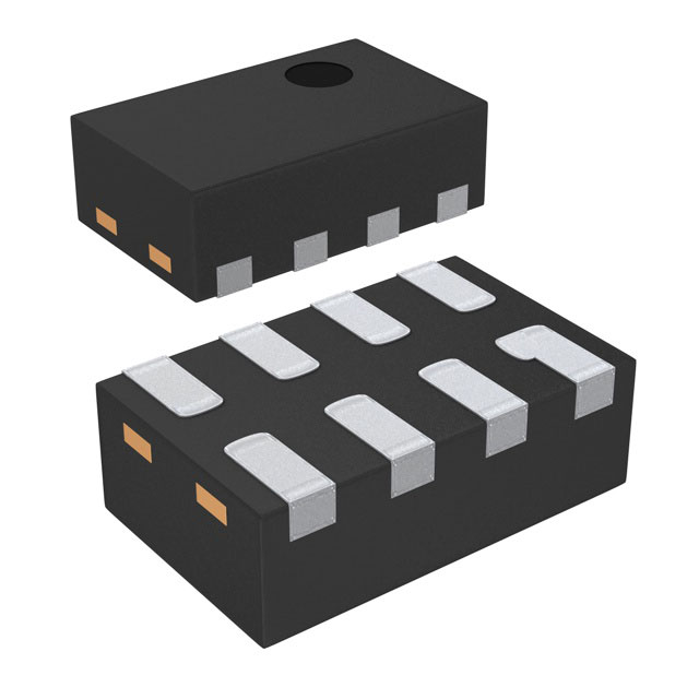
• 1.0 x 1.6 x 0.55 mm FC-STDFN package (2 fused pins for
drain and 2 fused pins for source)
• Logic level ON pin capable of supporting 0.85 V CMOS
Logic
• Discharged Load when off
• Fast Turn On time
• 32 μs, CSLEW = 0.1 nF, CLOAD = 1 μF, IDS = 100 mA
• 102 μs, CSLEW = 0.5 nF, CLOAD = 10 μF, IDS = 2.5 A
• Low RDSON while supporting 2.5 A
• 20 mΩ, VDD = 5 V, VD = 1 V
• 27.5 mΩ, VDD = 3.3 V, VD = 1 V
• Pb-Free / Halogen-Free / RoHS compliant
• Operating Temperature: -40 °C to 85°C
• Operating Voltage: 2.5 V to 5.5 V
• Power Rail Switching VD = 0.85 V to VD = VDD - 1.5 V
VDD
1
ON
2
D
3
D
4
SLG5NT1533V
The SLG5NT1533V is a 20 mΩ 2.5 A single-channel load
switch with configurable slew rate control. The device can
enable fast power rail turn on with big cap loading. Internal
circuit limits max inrush current to prevent device damage. The
product is packaged in an ultra-small 1.0 x 1.6 mm package.
8
GND
7
CAP
6
S
5
S
8-pin FC-STDFN
(Top View)
Applications
• Fast Turn On/Off power rail switching with big load
capacitance
• Frequent wake & sleep power cycle
• Mobile devices and portable devices
Block Diagram
2.5 A @ 20 mΩ
D
S
CIN
CLOAD
VDD
+2.5 V to 5.5 V
CSLEW
ON
Datasheet
CFR0011-120-01
Input
Circuit
Revision 1.07
Page 1 of 15
3-Feb-2022
©2022 Renesas Electronics Corporation
�����
SLG5NT1533V
20 mΩ, Fast Turn On, 2.5 A
Load Switch with Discharge
Pin Description
Pin #
Pin Name
Type
Pin Description
1
VDD
PWR
VDD supplies the power for the operation of the load switch and internal control circuitry.
Bypass the VDD pin to GND with a 0.1 µF (or larger) capacitor.
2
ON
Input
A low-to-high transition on this pin initiates the operation of the SLG5NT1533V’s state
machine. ON is a CMOS input with ON_VIL < 0.3 V and ON_VIH > 0.85 V thresholds. While
there is an internal pull-down circuit to GND (~4 MΩ), connect this pin directly to a
general-purpose output (GPO) of a microcontroller, an application processor, or a system
controller.
3, 4
D
MOSFET
Drain terminal connection of the n-channel MOSFET (2 pins fused for VD). Connect at least
a low-ESR 0.1 µF capacitor from this pin to ground. Capacitors used at VD should be rated
at 10 V or higher.
5, 6
S
MOSFET
Source terminal connection of the n-channel MOSFET (2 pins fused for VS). Connect a
low-ESR capacitor from this pin to ground and consult the Electrical Characteristics table
for recommended CLOAD range. Capacitors used at VS should be rated at 10 V or higher.
7
CAP
Input
A low-ESR, stable dielectric, ceramic surface-mount capacitor connected from CAP pin to
GND sets the VS slew rate and overall turn-on time of the SLG5NT1533V. Capacitors at
CAP pin should be rated at 10 V or higher.
8
GND
GND
Ground connection. Connect this pin to system analog or power ground plane.
Ordering Information
Part Number
Type
Production Flow
SLG5NT1533V
FC-STDFN 8L
Industrial, -40 °C to 85 °C
SLG5NT1533VTR
FC-STDFN 8L (Tape and Reel)
Industrial, -40 °C to 85 °C
Datasheet
CFR0011-120-01
Revision 1.07
Page 2 of 15
3-Feb-2022
©2022 Renesas Electronics Corporation
�����
SLG5NT1533V
20 mΩ, Fast Turn On, 2.5 A
Load Switch with Discharge
Absolute Maximum Ratings
Parameter
VDD
Description
Conditions
Min.
Typ.
Max.
Unit
--
--
7
V
Power Supply
VD to GND
Load Switch Input Voltage to GND
-0.3
--
VDD
V
VS to GND
Load Switch Output Voltage to
GND
-0.3
--
VD
V
-0.3
--
VDD
V
ON and CAP to
ON and CAP Pin Voltages to GND
GND
TS
Storage Temperature
-65
--
150
°C
TJ
Junction Temperature
--
--
150
°C
2000
--
--
V
--
°C/W
ESDHBM
MSL
θJA
WDIS
ESD Protection
Human Body Model
Moisture Sensitivity Level
Thermal Resistance
1
1.6 x 1 mm, 8L STDFN; Determined using
1 in2, 1 oz. copper pads under each VD
and VS terminals and FR4 pcb material
Package Power Dissipation
--
75
--
--
0.4
W
For no more than 20 μs with 1% duty cycle
--
--
25.0
A
MOSFET IDSPK Peak Current from Drain to Source For no more than 50 μs with 1% duty cycle
--
--
12.5
A
For no more than 1 ms with 1% duty cycle
--
--
3.5
A
Note: Stresses greater than those listed under “Absolute Maximum Ratings” may cause permanent damage to the device. This is a stress rating
only and functional operation of the device at these or any other conditions above those indicated in the operational sections of this
specification is not implied. Exposure to absolute maximum rating conditions for extended periods may affect reliability.
Electrical Characteristics
TA = -40 °C to 85 °C. Typical values are at TA = 25 °C unless otherwise noted.
Parameter
VDD
IDD
Description
Power Supply Voltage
Power Supply Current (PIN 1)
ON Resistance, TA = 25°C
RDSON
ON Resistance, TA = 70°C
ON Resistance, TA = 85°C
MOSFET IDS Current from D to S
VD
Datasheet
CFR0011-120-01
Conditions
-40 °C to 85 °C
Min.
Typ.
Max.
Unit
2.5
--
5.5
V
when OFF
--
--
1
μA
when ON, No load
--
--
10
μA
VDD = 5 V, VD = 1.0 V,
VDD - VD = 4.0 V, RLOAD = 0.5 Ω
--
20
24
mΩ
VDD = 3.3 V, VD = 1.0 V,
VDD - VD = 2.3 V, RLOAD = 0.5 Ω
--
27.5
31
mΩ
VDD = 5 V, VD = 1.0 V,
VDD - VD = 4.0 V, RLOAD = 0.5 Ω
--
23.5
27
mΩ
VDD = 3.3 V, VD = 1.0 V,
VDD - VD = 2.3 V, RLOAD = 0.5 Ω
--
31
35
mΩ
VDD = 5 V, VD = 1.0 V,
VDD - VD = 4.0 V, RLOAD = 0.5 Ω
--
24.5
28
mΩ
VDD = 3.3 V, VD = 1.0 V,
VDD - VD = 2.3 V, RLOAD = 0.5 Ω
--
33
37
mΩ
Continuous, VD = 0.85 V to 3.3 V
--
--
2.5
A
0.85
--
VDD
- 1.5
V
Drain Voltage
Revision 1.07
Page 3 of 15
3-Feb-2022
©2022 Renesas Electronics Corporation
�����
SLG5NT1533V
20 mΩ, Fast Turn On, 2.5 A
Load Switch with Discharge
Electrical Characteristics (continued)
TA = -40 °C to 85 °C. Typical values are at TA = 25 °C unless otherwise noted.
Parameter
TON_Delay
Description
ON Delay Time
Min.
Typ.
Max.
Unit
50% ON to 10% VS,
VDD = 5 V, VD = 1.0 V, CSLEW = 0.1 nF
Conditions
--
12
15
μs
50% ON to 10% VS,
VDD = 5 V, VD = 1.0 V, CSLEW = 0.5 nF
--
32
35
μs
50% ON to 90% VS
TTotal_ON
Total Turn On Time
CLOAD
RDISCHRGE
Slew Rate
Output Load Capacitance
μs
50% ON to 90% VS, VDD = 5 V,
VD = 1.0 V, CLOAD = 1 μF,
IDS = 50 mA, CSLEW = 0.1 nF
--
32
39
μs
50% ON to 90% VS, VDD = 5 V,
VD = 1.0 V, CLOAD = 1 μF,
IDS = 100 mA, CSLEW = 0.1 nF
--
32
39
μs
50% ON to 90% VS, VDD = 5 V,
VD = 1.0 V, CLOAD = 4.7 μF,
IDS = 2.5 A, CSLEW = 0.5 nF
--
102
123
μs
50% ON to 90% VS, VDD = 5 V,
VD = 1.0 V, CLOAD = 10 μF,
IDS = 2.5 A, CSLEW = 0.5 nF
--
102
123
μs
10% VS to 90% VS
VS(SR)
Set by External CSLEW1
Set by External CSLEW1
V/ms
10% VS to 90% VS, VDD = 5 V,
VD = 1.0 V, CLOAD = 1 μF,
IDS = 50 mA, CSLEW = 0.1 nF
--
65
78
V/ms
10% VS to 90% VS, VDD = 5 V,
VD = 1.0 V, CLOAD = 1 μF,
IDS = 100 mA, CSLEW = 0.1 nF
--
65
78
V/ms
10% VS to 90% VS, VDD = 5 V,
VD = 1.0 V, CLOAD = 4.7 μF,
IDS = 2.5 A, CSLEW = 0.5 nF
--
13
16
V/ms
10% VS to 90% VS, VDD = 5 V,
VD = 1.0 V, CLOAD = 10 μF,
IDS = 2.5 A, CSLEW = 0.5 nF
--
13.5
16.5
V/ms
CLOAD connected from S to GND
--
--
10
μF
Discharge Resistance
100
150
300
Ω
ON_VIH
High Input Voltage on ON pin
0.85
--
VDD
V
ON_VIL
Low Input Voltage on ON pin
-0.3
0
0.3
V
TOFF_Delay
OFF Delay Time
50% ON to VS Fall Start, no CLOAD,
RLOAD = 20 Ω, VDD = 5 V, VD = 1.0 V,
No CSLEW
--
120
150
μs
THERMOFF
Thermal shutoff turn-off temperature
Programmable, automatic shutoff
temperature
--
125
--
°C
--
--
±20
%
--
--
100
μs
THERMOFFACC Thermal Sensor Accuracy
THERMDT
Thermal Disable Time
Thermal sensor disable for the ON
rising edge to 100 μs. Prevent thermal
shutdown from inrush current
Notes:
1. Refer to typical timing parameter vs. CSLEW performance charts for additional information when available.
Datasheet
CFR0011-120-01
Revision 1.07
Page 4 of 15
3-Feb-2022
©2022 Renesas Electronics Corporation
�����
SLG5NT1533V
20 mΩ, Fast Turn On, 2.5 A
Load Switch with Discharge
TON_Delay, VS(SR), and TTotal_ON Timing Details
ON*
50% ON
50% ON
TOFF_Delay
90% VS
VS
90% VS
TON_Delay
10% VS
10% VS
VS(SR) (V/ms)
TFALL
TTotal_ON
Note: * Rise and Fall times of the ON signal are 100 ns
Datasheet
CFR0011-120-01
Revision 1.07
Page 5 of 15
3-Feb-2022
©2022 Renesas Electronics Corporation
�����
SLG5NT1533V
20 mΩ, Fast Turn On, 2.5 A
Load Switch with Discharge
Typical Performance Characteristics
RDSON vs. Temperature and VDD - VD
RDSON vs. VDD - VD
Datasheet
CFR0011-120-01
Revision 1.07
Page 6 of 15
3-Feb-2022
©2022 Renesas Electronics Corporation
�����
SLG5NT1533V
20 mΩ, Fast Turn On, 2.5 A
Load Switch with Discharge
VS Slew Rate vs. CSLEW
TTotal_ON vs. CSLEW
Datasheet
CFR0011-120-01
Revision 1.07
Page 7 of 15
3-Feb-2022
©2022 Renesas Electronics Corporation
�����
SLG5NT1533V
20 mΩ, Fast Turn On, 2.5 A
Load Switch with Discharge
SLG5NT1533V Power-Up/Power-Down Sequence Considerations
A nominal power-up sequence is to apply VDD first, followed by VD only after VDD is > 90 % of final VDD, and finally toggling the
ON pin LOW-to-HIGH after VD is at least 90% of its final value.
A nominal power-down sequence is the power-up sequence in reverse order.
If VDD and VD are applied at the same time, a voltage glitch may appear on the output pin at VS. To prevent glitches at the output,
it is recommended to connect at least a 1 μF capacitor from the S pin to GND and to keep the VDD and VD ramp times higher
than 2 ms.
If the ON pin is toggled HIGH before VDD and VD have reached their steady-state values the load switch timing parameters may
differ from datasheet specifications.
Power Dissipation
The junction temperature of the SLG5NT1533V depends on different factors such as board layout, ambient temperature, and
other environmental factors. The primary contributor to the increase in the junction temperature of the SLG5NT1533V is the power
dissipation of its power MOSFET. Its power dissipation and the junction temperature in nominal operating mode can be calculated
using the following equations:
PD = (RDSON x IDS2) + (VDD x IDD)
where:
PD = Power dissipation, in Watts (W)
RDSON = Power MOSFET ON resistance, in Ohms (Ω)
IDS = Output current, in Amps (A)
VDD = Power supply voltage applied to the SLG5NT1533V, in Volts (V)
IDD = Power supply current of the SLG5NT1533V at VDD, in Amps (A)
and
TJ = PD x θJA + TA
where:
TJ = Junction temperature, in Celsius degrees (°C)
θJA = Package thermal resistance, in Celsius degrees per Watt (°C/W) = 75 °C/W for the SLG5NT1533V’s STDFN package.
TA = Ambient temperature, in Celsius degrees (°C)
For more information on GreenFET load switch features, please visit our website and see App Note “AN-1068 GreenFET and
High Voltage GreenFET Load Switch Basics”.
Datasheet
CFR0011-120-01
Revision 1.07
Page 8 of 15
3-Feb-2022
©2022 Renesas Electronics Corporation
�����
SLG5NT1533V
20 mΩ, Fast Turn On, 2.5 A
Load Switch with Discharge
Layout Guidelines:
1. The VDD pin needs a 0.1µF (or larger) external capacitor to smooth pulses from the power supply. Locate this capacitor as
close as possible to the SLG5NT1533V's pin 1.
2.Since the D and S pins dissipate most of the heat generated during high-load current operation, it is highly recommended to
make power traces as short, direct, and wide as possible. A good practice is to make power traces with absolute minimum
widths of 15 mils (0.381 mm) per Ampere. A representative layout, shown in Figure 1, illustrates proper techniques for heat to
transfer as efficiently as possible out of the device;
3.To minimize the effects of parasitic trace inductance on normal operation, it is recommended to connect input CIN and output
CLOAD low-ESR capacitors as close as possible to the SLG5NT1533V's D and S pins;
4.The GND pin should be connected to system analog or power ground plane.
5. 2 oz. copper is recommended for high current operation.
SLG5NT1533V Evaluation Board:
А GFET3 Evaluation Board for SLG5NT1533V is designed according to the statements above and is illustrated on Figure 1.
Please note that evaluation board has D_Sense and S_Sense pads. They cannot carry high currents and dedicated only for
RDSON evaluation.
Please solder your SLG5NT1533V here
Figure 1. SLG5NT1533V Evaluation Board
Datasheet
CFR0011-120-01
Revision 1.07
Page 9 of 15
3-Feb-2022
©2022 Renesas Electronics Corporation
�����
SLG5NT1533V
20 mΩ, Fast Turn On, 2.5 A
Load Switch with Discharge
1
1
VDD
C2
1
2
3
4
5
VDD CAP2
GND CAP1
ON1
S2
ON2
S1
D1
D2
C1
10
9
8
7
6
CAP/RILIM
ON
U1
1
2
3
D_Sense1
1
2
3
4
1
VDD
ON
D
D
C3
C4
1
3
5
7
9
S_Sense1
1
C5
C6
R1
2
4
6
8
10
R2
R3
R4
C7
1 00 n
R_Array
1
3
5
7
9
8
7
6
5
GND
CAP
S
S
2
4
6
8
10
U2
9
1
2
3
4
D_Sense2
ON
VDD
D
D
D
8
7
6
5
GND
CAP
S
S
S_Sense2
1
1
C8
1 00 n
U3
1
2
3
4
D_Sense3
ON
VDD
D
D
8
7
6
5
GND
CAP
S
S
S_Sense3
1
1
C9
1 00 n
U4
9
1
2
3
4
D_Sense4
1
ON
VDD
D
D
D
8
7
6
5
GND
S
S
S
S_Sense4
1
U5
1
2
3
4
D_Sense5
1
ON
VIN
VIN
VIN
8
7
6
5
GND
VOUT
VOUT
VOUT
S_Sense5
1
U6
1
2
ON
D
GN D
S
4
3
D_Sense6
1
1
1
D/VIN
D/VIN
1
S_Sense6
1
1
S/VOUT S/VOUT
Figure 2. SLG5NT1533V Evaluation Board Connection Circuit
Datasheet
CFR0011-120-01
Revision 1.07
Page 10 of 15
3-Feb-2022
©2022 Renesas Electronics Corporation
�����
SLG5NT1533V
20 mΩ, Fast Turn On, 2.5 A
Load Switch with Discharge
Basic Test Setup and Connections
Figure 3. SLG5NT1533V Evaluation Board Connection Circuit
EVB Configuration
1. Connect oscilloscope probes to D/VIN, S/VOUT, ON, etc.;
2. Turn on Power Supply 1 and set desired VDD from 2.5 V…5.5 V range;
3. Turn on Power Supply 2 and set desired VD from 0.85 V…VDD - 1.5 V range;
4 .Toggle the ON signal High or Low to observe SLG5NT1533V operation.
Datasheet
CFR0011-120-01
Revision 1.07
Page 11 of 15
3-Feb-2022
©2022 Renesas Electronics Corporation
�����
SLG5NT1533V
20 mΩ, Fast Turn On, 2.5 A
Load Switch with Discharge
Package Top Marking System Definition
ABC
Serial Number
Pin 1 Identifier
Each character in Serial Number field can be alphanumeric A-Z
Datasheet
CFR0011-120-01
Revision 1.07
Page 12 of 15
3-Feb-2022
©2022 Renesas Electronics Corporation
�����
SLG5NT1533V
20 mΩ, Fast Turn On, 2.5 A
Load Switch with Discharge
Package Drawing and Dimensions
8 Lead STDFN Package 1.0 x 1.6 mm (Fused Lead)
Datasheet
CFR0011-120-01
Revision 1.07
Page 13 of 15
3-Feb-2022
©2022 Renesas Electronics Corporation
�����
SLG5NT1533V
20 mΩ, Fast Turn On, 2.5 A
Load Switch with Discharge
Tape and Reel Specifications
Max Units
Leader (min)
Nominal
Reel &
Package # of
Package Size
Hub Size
Length
Type
Pins
per Reel per Box
Pockets
[mm]
[mm]
[mm]
STDFN 8L
1x1.6mm
0.4P FC
Green
8
1.0 x 1.6 x 0.55
3,000
3,000
178 / 60
100
400
Trailer (min)
Pockets
Length
[mm]
Tape
Width
[mm]
100
400
8
Part
Pitch
[mm]
4
Carrier Tape Drawing and Dimensions
Pocket BTM Pocket BTM
Package
Length
Width
Type
STDFN 8L
1x1.6mm
0.4P FC
Green
Pocket
Depth
Index Hole
Pitch
Pocket
Pitch
Index Hole
Diameter
Index Hole Index Hole
to Tape
to Pocket Tape Width
Edge
Center
A0
B0
K0
P0
P1
D0
E
F
W
1.12
1.72
0.7
4
4
1.55
1.75
3.5
8
Recommended Reflow Soldering Profile
Please see IPC/JEDEC J-STD-020: latest revision for reflow profile based on package volume of 0.88 mm3 (nominal). More
information can be found at www.jedec.org.
Datasheet
CFR0011-120-01
Revision 1.07
Page 14 of 15
3-Feb-2022
©2022 Renesas Electronics Corporation
�����
SLG5NT1533V
20 mΩ, Fast Turn On, 2.5 A
Load Switch with Discharge
Revision History
Date
Version
Change
2/3/2022
1.07
Updated Company name and logo
Fixed typos
11/26/2018
1.06
Added Junction Temperature to Abs Max Table
11/8/2018
1.05
Updated Style and formatting
Updated Abs, Max and Electrical Characteristics tables
Added Applications information
Added Layout Guidelines
8/14/2015
1.04
Add support for 0.85 VD
4/22/2015
1.03
Removed TBD from Timing Diagram
4/20/2015
1.02
Fixed Block Diagram (added Discharge Resistor)
9/15/2014
1.01
Added MSL
6/16/2014
1.0
Production release
Datasheet
CFR0011-120-01
Revision 1.07
Page 15 of 15
3-Feb-2022
©2022 Renesas Electronics Corporation
�IMPORTANT NOTICE AND DISCLAIMER
RENESAS ELECTRONICS CORPORATION AND ITS SUBSIDIARIES (“RENESAS”) PROVIDES TECHNICAL
SPECIFICATIONS AND RELIABILITY DATA (INCLUDING DATASHEETS), DESIGN RESOURCES (INCLUDING
REFERENCE DESIGNS), APPLICATION OR OTHER DESIGN ADVICE, WEB TOOLS, SAFETY INFORMATION, AND
OTHER RESOURCES “AS IS” AND WITH ALL FAULTS, AND DISCLAIMS ALL WARRANTIES, EXPRESS OR IMPLIED,
INCLUDING, WITHOUT LIMITATION, ANY IMPLIED WARRANTIES OF MERCHANTABILITY, FITNESS FOR A
PARTICULAR PURPOSE, OR NON-INFRINGEMENT OF THIRD PARTY INTELLECTUAL PROPERTY RIGHTS.
These resources are intended for developers skilled in the art designing with Renesas products. You are solely responsible
for (1) selecting the appropriate products for your application, (2) designing, validating, and testing your application, and (3)
ensuring your application meets applicable standards, and any other safety, security, or other requirements. These
resources are subject to change without notice. Renesas grants you permission to use these resources only for
development of an application that uses Renesas products. Other reproduction or use of these resources is strictly
prohibited. No license is granted to any other Renesas intellectual property or to any third party intellectual property.
Renesas disclaims responsibility for, and you will fully indemnify Renesas and its representatives against, any claims,
damages, costs, losses, or liabilities arising out of your use of these resources. Renesas' products are provided only subject
to Renesas' Terms and Conditions of Sale or other applicable terms agreed to in writing. No use of any Renesas resources
expands or otherwise alters any applicable warranties or warranty disclaimers for these products.
(Rev.1.0 Mar 2020)
Corporate Headquarters
Contact Information
TOYOSU FORESIA, 3-2-24 Toyosu,
Koto-ku, Tokyo 135-0061, Japan
www.renesas.com
For further information on a product, technology, the most
up-to-date version of a document, or your nearest sales
office, please visit:
www.renesas.com/contact/
Trademarks
Renesas and the Renesas logo are trademarks of Renesas
Electronics Corporation. All trademarks and registered
trademarks are the property of their respective owners.
© 2021 Renesas Electronics Corporation. All rights reserved.
�