TS79M00 Series
Taiwan Semiconductor
3-Termal 500mA Negative Voltage Regulator
FEATURES
The TS79M00 series of fixed output negative voltage
●
Output Voltage: -5 & -12V
regulators are intended as complements to the popular
●
Output current up to 0.5A
TS78M00 series device. These negative regulators are
●
No external components required
available in the same seven-voltage options as the
●
Internal thermal overload protection
TS7900 devices. In addition, one extra voltage option
●
Internal short-circuit current limiting
commonly employed in MECL systems is also available
●
●
●
Output transistor safe-area compensation
Output voltage offered in 4% tolerance
Compliant to RoHS Directive 2011/65/EU and
WEEE 2002/96/EC
Halogen-free according to IEC 61249-2-21
in the negative TS79M00 Series. Available in fixed
output voltage options from -5.0 and -12 volts, these
en
de
d
DESCRIPTION
regulators employ current limiting, thermal shutdown,
and safe-area compensation--making them remarkably
rugged under most operating conditions. With adequate
heat sinking they can deliver output currents in excess
APPLICATION
●
Switching power supply
●
Home appliance
mm
of 0.5 ampere.
●
TO-252
(DPAK)
Pin Definition:
1. Ground
2. Input (tab)
3. Output
tR
eco
TO-220
Notes: MSL 3 (Moisture Sensitivity Level) per J-STD-020
No
TYPICAL APPLICATION CIRCUIT
A common ground is required between the input and the output voltages. The input voltage must remain typically 2V above
the output voltage even during the low point on the Input ripple voltage.
XX = these two digits of the type number indicate voltage.
* = CIN is required if regulator is located an appreciable distance from power supply filter.
** = COUT is not needed for stability; however, it does improve transient response.
1
Version: F1603
�TS79M00 Series
Taiwan Semiconductor
ABSOLUTE MAXIMUM RATINGS
PARAMETER
SYMBOL
LIMIT
UNIT
Input Voltage
VIN
-35
V
Power Dissipation
PD
Internal Limited
Operating Junction Temperature
0~+125
-65~+150
o
TJ
Storage Temperature Range
TSTG
W
o
C
C
THERMAL PERFORMANCE
LIMIT
Junction to Case Thermal Resistance
RӨJC
Junction to Ambient Thermal Resistance
RӨJA
UNIT
d
SYMBOL
TO-220
TO-252
5
6
°C/W
65
92
°C/W
de
PARAMETER
Notes: RӨJA is the sum of the junction-to-case and case-to-ambient thermal resistances. The case thermal reference is defined
en
at the solder mounting surface of the drain pins. RӨJA is guaranteed by design while RӨCA is determined by the user’s board
design. RӨJA shown below for single device operation on FR-4 PCB in still air.
o
o
mm
ELECTRICAL SPECIFICATIONS TS79M05
(VIN=-10V, IOUT=350mA, 0 C≤TJ≤125 C, CIN=0.33µF, COUT=0.1µF, unless otherwise noted)
PARAMETER
CONDITIONS
o
TJ=25 C
Line Regulation
o
TJ=25 C
o
TJ=25 C
-7.5V≤VIN≤-25V
-8V≤VIN≤-18V
5mA≤IOUT≤500mA
5mA≤IOUT≤200mA
tR
Load Regulation
-7.5V≤VIN≤-20V,
5mA≤IOUT≤500mA, PD≤5W
VOUT
e co
Output voltage
SYMBOL
Quiescent Current
REGLOAD
TYP
MAX
-4.80
-5
-5.20
-4.75
-5
-5.25
--
7
50
--
2
30
--
20
100
--
10
50
IOUT=0, TJ=25 C
IQ
--
4
8
-7.5V≤VIN≤-25V
ΔIQ
--
--
1
--
--
0.5
5mA≤IOUT≤500mA
No
Quiescent Current Change
o
REGLINE
MIN
o
UNIT
V
mV
mA
Output Noise Voltage
10Hz≤f≤100kHz, TJ=25 C
VN
--
40
--
µV
Ripple Rejection Ratio
f=120Hz, -8V≤VIN≤-18V
RR
54
66
--
dB
VDROP
--
2
--
V
Io peak
--
2.1
--
A
ΔVOUT/ ΔTJ
--
-0.1
--
mV/ C
Voltage Drop
o
IOUT=500mA, TJ=25 C
o
Peak Output Current
TJ=25 C
Temperature Coefficient of
Output Voltage
IOUT=5mA, 0 C≤TJ≤125 C
o
o
2
o
Version: F1603
�TS79M00 Series
Taiwan Semiconductor
ELECTRICAL SPECIFICATIONS TS79M12
o
o
(VIN=-19V, IOUT=350mA, 0 C≤TJ≤125 C, CIN=0.33µF, COUT=0.1µF, unless otherwise noted)
CONDITIONS
SYMBOL
o
TJ=25 C
Output voltage
-14.5V≤VIN≤-27V,
5mA≤IOUT≤500mA, PD≤5W
Line Regulation
TJ=25 C
o
o
Load Regulation
TJ=25 C
VOUT
-14.5V≤VIN≤-30V
-15V≤VIN≤-19V
5mA≤IOUT≤500mA
-12
-12.48
-11.42
-12
-12.60
--
10
240
--
3
120
--
12
240
--
4
120
--
4.3
8
de
-14.5V≤VIN≤-30V
Ripple Rejection Ratio
f=120Hz, -15V≤VIN≤-25V
o
Peak Output Current
TJ=25 C
Temperature Coefficient of
Output Voltage
IOUT=5mA, 0 C≤TJ≤125 C
o
o
mV
mA
1
--
--
0.5
VN
--
75
--
µV
RR
55
70
--
dB
VDROP
--
2
--
V
Io peak
--
2.1
--
A
ΔVOUT/ ΔTJ
--
-1
--
mV/ C
mm
IOUT=500mA, TJ=25 C
V
--
en
o
10Hz≤f≤100kHz, TJ=25 C
UNIT
--
ΔIQ
5mA≤IOUT≤500mA
o
-11.53
IQ
Output Noise Voltage
Voltage Drop
MAX
REGLOAD
5mA≤IOUT≤200mA
IOUT=0, TJ=25 C
Quiescent Current Change
TYP
REGLINE
o
Quiescent Current
MIN
d
PARAMETER
o
e co
Note:
1. Pulse testing techniques are used to maintain the junction temperature as close to the ambient temperature as possible,
and thermal effects must be taken into account separately
2. This specification applies only for DC power dissipation permitted by absolute maximum ratings.
tR
ORDERING INFORMATION
OUTPYT VOLTAGE
PACKAGE
PACKING
TS79M05CZ C0G
TO-220
50pcs / Tube
TS79M05CP ROG
TO-252
2,500pcs / 13” Reel
TS79M12CP ROG
TO-252
2,500pcs / 13” Reel
No
5V
PART NO.
12V
3
Version: F1603
�TS79M00 Series
Taiwan Semiconductor
de
d
CHARACTERISTICS CURVES
e co
mm
en
Figure 1. Worse Case Power Dissipation vs. Ambient Figure 2. Peak Output Current as a Function of InputTemperature (TO-220)
Output Differential Voltage
Figure 4. Bias Current vs. Output Current
No
tR
Figure 3. Bias Current vs. Input Voltage
Figure 5. Ripple Rejection vs. Frequency
Figure 6. Ripple Rejection vs. Output Voltage
4
Version: F1603
�TS79M00 Series
Taiwan Semiconductor
de
d
APPLICATION INFORMATION
Figure 7. DPAK Thermal Resistance and Maximum
No
tR
e co
mm
en
Power Dissipation vs. P.C.B Copper Length
5
Version: F1603
�TS79M00 Series
Taiwan Semiconductor
PACKAGE OUTLINE DIMENSIONS (Unit: Millimeters)
MARKING DIAGRAM
e co
XX = Output Voltage
mm
en
de
d
TO-220
No
tR
05 =-5V
Y = Year Code
M = Month Code for Halogen Free Product
O =Jan P =Feb Q =Mar R =Apr
S =May T =Jun U =Jul
V =Aug
W =Sep X =Oct
Y =Nov Z =Dec
L = Lot Code
CZ = Package code
6
Version: F1603
�TS79M00 Series
Taiwan Semiconductor
PACKAGE OUTLINE DIMENSIONS (Unit: Millimeters)
tR
e co
mm
SUGGESTED PAD LAYOUT (Unit: Millimeters)
en
de
d
TO-252 (DPAK)
No
MARKING DIAGRAM
XX = Output Voltage
05 =-5V 12 =-12V
Y = Year Code
M = Month Code for Halogen Free Product
O =Jan P =Feb Q =Mar R =Apr
S =May T =Jun U =Jul
V =Aug
W =Sep X =Oct
Y =Nov Z =Dec
L = Lot Code
CP = Package code
7
Version: F1603
�TS79M00 Series
No
tR
e co
mm
en
de
d
Taiwan Semiconductor
Notice
Specifications of the products displayed herein are subject to change without notice. TSC or anyone on its behalf,
assumes no responsibility or liability for any errors or inaccuracies.
Information contained herein is intended to provide a product description only. No license, express or implied, to
any intellectual property rights is granted by this document. Except as provided in TSC’s terms and conditions of
sale for such products, TSC assumes no liability whatsoever, and disclaims any express or implied warranty,
relating to sale and/or use of TSC products including liability or warranties relating to fitness for a particular purpose,
merchantability, or infringement of any patent, copyright, or other intellectual property right.
The products shown herein are not designed for use in medical, life-saving, or life-sustaining applications.
Customers using or selling these products for use in such applications do so at their own risk and agree to fully
indemnify TSC for any damages resulting from such improper use or sale.
8
Version: F1603
�
很抱歉,暂时无法提供与“TS79M05CZ C0G”相匹配的价格&库存,您可以联系我们找货
免费人工找货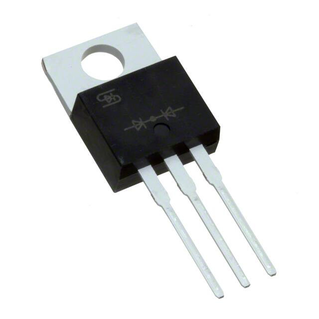


 工商网监
湘ICP备2023018690号
工商网监
湘ICP备2023018690号
